Op-amp circuits use negative feedback to turn a very high-gain differential amplifier into amplifiers, summers, integrators, converters, precision rectifiers and log amplifiers. Their behaviour is set only by the external components, through the virtual short that the feedback creates. To solve these questions you apply that short correctly with KCL at the inverting node, recognise when it does not hold, and correct the ideal result for finite gain, gain-bandwidth product, slew rate, offsets and CMRR. EC candidates also need dominant-pole (Miller) compensation and phase margin.
36 previous-year questions · 36 solved · 6 practice questions
The ideal op-amp, the virtual short and the node method
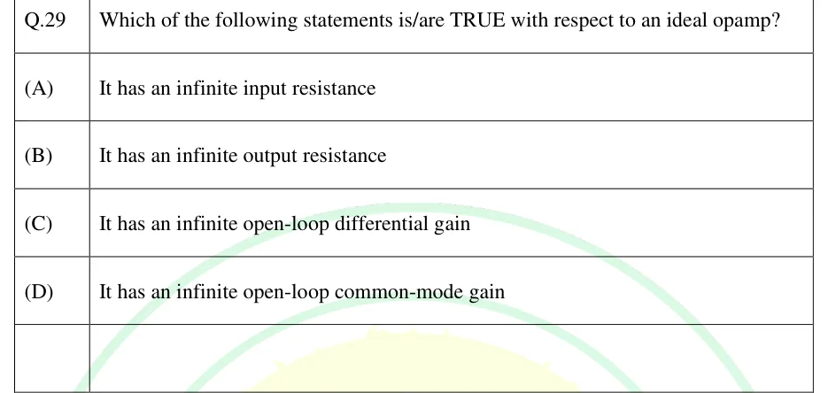
An op-amp amplifies the difference between its two inputs: vo=A(v+−v−). Unless a finite value is given, these notes use the ideal op-amp: open-loop gain A→∞, input resistance Ri→∞ (no current into either input), output resistance Ro=0, infinite bandwidth and slew rate, zero offset voltage and bias current, and infinite CMRR. The output can swing only between ±Vsat, just inside the supply rails.
OPEN-LOOP RELATION AND VIRTUAL SHORT
vo=A(v+−v−),v+−v−=Avo→0as A→∞
The input difference goes to zero only when negative feedback holds the output at a finite value inside ±Vsat.
With negative feedback the output settles wherever it has to so that v−=v+. This is the virtual short. It is an equality of voltages only: no current flows between the inputs. When v+ is grounded, v− sits at 0 V and is called a virtual ground. Because Ro=0, the output can source or sink whatever current the circuit demands. KCL at the op-amp output node therefore only brings in the op-amp's own output current as an extra unknown, so do not use it to find vo; write KCL at the inverting node instead.
Node method for any linear op-amp circuit
Check that the net feedback goes to the inverting input. If it does not, stop: the virtual short does not apply.
Find v+ from the network on the non-inverting side. No current enters the input, so a plain voltage divider (or weighted average) gives it. If that network is also connected to vo, keep vo in the expression.
Set v−=v+.
Write KCL at the inverting node with zero current into the op-amp.
Solve for vo. With several sources, superposition works because the circuit is linear.
When the virtual short does NOT hold
Situation
What happens
How to analyse
Open loop (comparator)
Output is +Vsat if v+>v− and −Vsat if v+<v−
Compare the two input voltages directly
Positive feedback only (Schmitt trigger, astable)
Output latches at ±Vsat;v+=v− except at the switching instant
Find v+ for each output state; the output switches when v− crosses it
Negative feedback but output saturated (overdriven amplifier, integrator at a rail, simple super diode on its off half-cycle)
The loop is broken, so the inputs are no longer equal
Treat the output as a fixed ±Vsat source
Output slewing
The output cannot follow; v+−v− is large during the edge
The output changes at the slew rate
Both positive and negative feedback
The net sign decides
With resistive networks the virtual short holds only if the fraction of vo returned to v− exceeds the fraction returned to v+
EXAM TIP
The feedback current enters the inverting node through the feedback element and then has nowhere to go but the other elements at that node, because the op-amp input draws nothing. Load current is supplied by the op-amp output and never appears in the inverting-node equation.
Linear amplifiers: inverting, non-inverting, summer, difference and instrumentation
Convention: R1 runs from the input (or ground) to the inverting node and Rf from the output to the inverting node. β=R1/(R1+Rf) is the feedback factor, and 1/β=1+Rf/R1 is the noise gain. It is the noise gain, not the signal gain, that later sets the bandwidth and multiplies the input offset voltage.
INVERTING AMPLIFIER
vivo=−R1Rf,Rin=R1,Rout=0
The input goes through R1 to the virtual-ground node, so the source sees only R1.
NON-INVERTING AMPLIFIER AND VOLTAGE FOLLOWER
vivo=1+R1Rf,Rin→∞
The input is at v+, with R1 from v− to ground. The gain is never below 1. With Rf=0 or R1→∞ this is the voltage follower, vo=vi, used as a buffer.
INVERTING SUMMER
vo=−Rf(R1v1+R2v2+⋯+Rnvn)
Each input sees only its own resistor because the summing node is a virtual ground, so the inputs do not interact. With all resistors equal, vo=−(v1+⋯+vn).
NON-INVERTING SUMMER
v+=∑k1/Rk∑kvk/Rk,vo=(1+RgRf)v+
The inputs go through Rk to v+ (with no other resistor at v+), which settles at their conductance-weighted average; Rg runs from v− to ground. Here the inputs do interact: changing one Rk changes every weight.
DIFFERENCE AMPLIFIER (GENERAL)
vo=−R1R2v1+(1+R1R2)R3+R4R4v2
v1 goes through R1 to v−, with R2 from the output to v−;v2 goes through R3 to v+, with R4 from v+ to ground. The result follows by superposition.
BALANCED DIFFERENCE AMPLIFIER
R3R4=R1R2⇒vo=R1R2(v2−v1)
The common-mode input cancels only with this ratio match. The differential input resistance is 2R1 when R3=R1 and R4=R2;v2 alone sees R3+R4.
DIFFERENCE AMPLIFIER WITH RESISTOR MISMATCH (IDEAL OP-AMP)
Here vd=v2−v1 and vcm=(v1+v2)/2. Any mismatch makes Acm=0, so resistor tolerance alone can limit the CMRR of this circuit even with a perfect op-amp.
The three-op-amp instrumentation amplifier puts a non-inverting buffer on each input, so neither input draws current, and follows them with a balanced difference amplifier. In the first stage, op-amp A1 (input v1 at its v+) and op-amp A2 (input v2) each have a resistor R from output to inverting input, and a single gain resistor RG joins the two inverting inputs. The virtual shorts put v2−v1 across RG, so the current (v2−v1)/RG flows through R,RG and R in series. The differential voltage is therefore amplified by 1+2R/RG. A common-mode voltage appears unchanged at both outputs, because no current flows in RG. The second stage (input resistors R3, feedback and ground resistors R4) amplifies vo2−vo1.
THREE-OP-AMP INSTRUMENTATION AMPLIFIER
vo=(1+RG2R)R3R4(v2−v1)
v2 drives the op-amp whose output feeds the non-inverting side of the difference stage. The gain is set by the single resistor RG without disturbing the matched R3 and R4. The first-stage outputs are vo1=v1−R(v2−v1)/RG and vo2=v2+R(v2−v1)/RG.
CURRENT-TO-VOLTAGE AND VOLTAGE-TO-CURRENT CONVERTERS
I-to-V: vo=−isRf,V-to-I (load ZL in place of Rf): iL=R1vi
I-to-V (transimpedance) converter: the source current is flows into the virtual-ground node and all of it goes through Rf, so the source sees zero resistance. V-to-I converter with a floating load: the load replaces Rf in an inverting amplifier, so the current vi/R1 flows through it from the inverting node towards the output whatever ZL is, as long as the output vo=−iLZL stays inside ±Vsat.
Linear configurations at a glance (ideal op-amp)
Circuit
Ideal gain
Resistance seen by the source
Noise gain 1/β
Inverting
−Rf/R1
R1
1+Rf/R1
Non-inverting
1+Rf/R1
∞
1+Rf/R1
Voltage follower
1
∞
1
Inverting summer, n inputs
−Rf/Rk per input
Rk per input
1+Rf/(R1∥⋯∥Rn)
Balanced difference
R2/R1 on (v2−v1)
2R1 differential (with R3=R1,R4=R2)
1+R2/R1
Instrumentation
(1+2R/RG)(R4/R3)
∞ at both inputs
—
EXAM TIP
An inverting amplifier with gain −1 still has a noise gain of 2. In the inverting and non-inverting forms alike, the noise gain 1+Rf/R1 multiplies VOS, and ft divided by the noise gain is the closed-loop bandwidth.
EXAM TIP
In the instrumentation amplifier with ideal first-stage op-amps, the first stage amplifies the difference by 1+2R/RG but passes the common-mode signal at unity gain, even if its two R resistors are not matched. The overall CMRR is therefore (1+2R/RG) times the CMRR of the difference stage alone.
Integrator and differentiator
Replace Rf in the inverting amplifier with a capacitor C, and the input current vi/R has nowhere to go but into C: the output is the negative running integral of the input. Swap the positions of R and C and the output becomes the negative derivative. Both results follow from the inverting-gain formula written with impedances, H=−Zf/Z1.
IDEAL INVERTING INTEGRATOR
vo(t)=−RC1∫0tvi(τ)dτ+vo(0),H(jω)=−jωRC1
∣H∣=1 at ω=1/(RC) and falls at 20 dB/decade. The phase is +90∘ (the output leads the input). The DC gain is infinite.
PRACTICAL INTEGRATOR (RF ACROSS C)
H(jω)=−1+jωRfCRf/R
It integrates only for f≫fc=1/(2πRfC). Below fc it is an inverting amplifier of gain −Rf/R, which stops offsets and bias currents from ramping the output into saturation.
INTEGRATOR WITH FINITE OPEN-LOOP GAIN A
H(jω)=−1+jω(1+A)RCA
The op-amp is ideal except for a frequency-independent gain A. The DC gain is −A instead of infinite, and the pole sits at ω=1/[(1+A)RC], because C appears at the inverting node multiplied by (1+A) (the Miller effect). Well above that pole the circuit integrates, and as A→∞ it reduces to −1/(jωRC).
IDEAL DIFFERENTIATOR
vo(t)=−RCdtdvi,H(jω)=−jωRC
∣H∣=1 at ω=1/(RC), and the gain rises at 20 dB/decade without limit. The phase is −90∘ (the output lags the input).
PRACTICAL DIFFERENTIATOR (R1 IN SERIES WITH C)
H(jω)=−1+jωR1CjωRC
It differentiates only for f≪1/(2πR1C), and the high-frequency gain is capped at −R/R1. A small capacitor across R is sometimes added to roll the gain off further.
INTEGRATOR OUTPUT FOR A SQUARE-WAVE INPUT
Δvo,pp=2RCVmT
For a zero-average square wave of ±Vm and period T, the output slopes at ∓Vm/(RC) for T/2 each half-cycle. A practical integrator needs RfC≫T for this to hold.
Standard input-output pairs (ideal circuits; for the sine, the steady-state output with the integration constant dropped)
Input
Integrator output
Differentiator output
Step of height V
Ramp of slope −V/(RC) until saturation
Impulse −RCVδ(t) (in practice a spike clipped at the rail), then 0
Square wave ±Vm, period T
Triangle, peak-to-peak VmT/(2RC)
Spikes of alternating sign at each edge
Triangle of slopes ±S
Piecewise parabola (close to a sine)
Square wave: −RCS while the input rises, +RCS while it falls
Vmsinωt
ωRCVmcosωt, amplitude ∝1/f
−ωRCVmcosωt, amplitude ∝f
WORKED EXAMPLE
A practical inverting integrator uses R=10kΩ,C=0.1μF and Rf=1MΩ across C. The input is a zero-average square wave of ±1 V at 1 kHz. The op-amp is ideal except for an input offset voltage VOS=2 mV. Find (a) the peak-to-peak output, (b) the DC level of the output, and (c) what happens if Rf is removed.
▸ Solution
Check that the circuit integrates at 1 kHz: fc=2πRfC1=2π(106)(10−7)1=1.59 Hz, far below 1 kHz, and RfC=0.1 s is much greater than T=1 ms.
RC=(104)(10−7)=1 ms. During each half-period T/2=0.5 ms the output slopes at Vm/(RC)=1 V/ms.
(a) Δvo,pp=2RCVmT=2(10−3)(1)(10−3)=0.5 V. The output is a triangle, falling while the input is +1 V and rising while it is −1 V.
(b) At DC the capacitor is open, so the circuit is an inverting amplifier with Rf/R=100 and noise gain 1+Rf/R=101. The output offset is 101×2mV=0.202 V, and the triangle rides on this level (its sign follows the sign of VOS).
(c) Without Rf the DC gain is infinite. With v+=v−=VOS, a constant current of magnitude VOS/R=0.2μA flows in R and therefore through C, so vo=VOS+RCVOSt. The output drifts at 2 V/s; taking the saturation level as 12 V, it saturates in about 6 s.
Answer: (a) A 0.5 V peak-to-peak triangle. (b) It rides on a DC level of about 0.2 V. (c) Without Rf the output drifts at 2 V/s until it saturates (about 6 s for a 12 V saturation level).
EXAM TIP
Sign check: both circuits invert. For vi=Vmsinωt the integrator gives +ωRCVmcosωt (the two minus signs cancel) and the differentiator gives −ωRCVmcosωt.
EXAM TIP
Why the ideal forms fail in practice. The ideal integrator's infinite DC gain integrates VOS and the bias current until the output saturates. The ideal differentiator's rising gain amplifies high-frequency noise, and its RC feedback network adds a pole to the loop that, together with the op-amp's own pole, leaves little phase margin, so the output rings. Rf in the integrator and R1 in the differentiator are the cures.
Precision rectifiers, log and antilog amplifiers
A diode on its own cannot rectify a signal smaller than its cut-in voltage Vγ. Putting the diode inside the feedback loop divides that dead zone by the open-loop gain. The diodes here can be ideal or constant-drop (0.7 V): either way the op-amp removes the drop from the output.
SUPER DIODE (DIODE INSIDE THE LOOP)
Vγ,eff=AVγ
A is the op-amp's open-loop gain. The op-amp output drives the diode anode. The cathode is the output node, which has a load resistor to ground and is fed back to v−;vi is at v+. The output is vo=vi for vi>0 and vo=0 (pulled down by the load) for vi<0. On the negative half the loop is open and the op-amp saturates at −Vsat, so it recovers slowly at high frequency.
The improved (inverting) precision half-wave rectifier adds a second diode so that the op-amp never saturates. It has input resistor R1 and feedback resistor R2. Diode D1 runs from v− (anode) to the op-amp output (cathode). Diode D2 runs from the op-amp output (anode) to the output node, and R2 connects the output node back to v−. For vi>0 the op-amp output goes negative, D1 conducts and clamps it one diode drop below ground, D2 is off, and the output node is held at the virtual ground through R2. For vi<0,D2 conducts and the circuit is an inverting amplifier.
IMPROVED PRECISION HALF-WAVE RECTIFIER (DIODES AS DESCRIBED)
vo=⎩⎨⎧−R1R2vi,0,vi<0vi>0
Reversing both diodes passes the other half-cycle: vo=−(R2/R1)vi for vi>0 and 0 otherwise. The op-amp output stays within about one diode drop of ground (while D1 conducts) or of the output node (while D2 conducts), so it never saturates and there is no saturation recovery.
The precision full-wave rectifier (absolute-value circuit) takes a half-wave rectifier of gain −1 that passes the positive half (vA=−vi for vi>0, otherwise 0; diodes reversed from the circuit above) and follows it with an inverting summer that weights vi by 1 and vA by 2 (input resistors R and R/2, feedback resistor R).
PRECISION FULL-WAVE RECTIFIER
vo=−(vi+2vA)=∣vi∣
For vi>0:vA=−vi, so vo=−(vi−2vi)=vi. For vi<0:vA=0, so vo=−vi. Reversing both diodes gives −∣vi∣.
A log amplifier puts a diode (or a BJT with its base grounded) in the feedback path. It uses the exponential diode law iD=ISevD/VT (the −1 term neglected, ideality factor 1), with VT=25 mV at room temperature unless stated. With the diode's anode at v− and an input resistor R, the input current vi/R flows through the diode and forces vD=−vo. Swapping R and the diode gives the antilog (exponential) amplifier.
LOG AMPLIFIER
vo=−VTln(ISRvi),vi>0
It works for one input polarity only (reverse the diode for vi<0). The output depends on temperature through both VT and IS. With a BJT (collector at v−, base grounded, emitter at the output), IS is the transistor's saturation current.
ANTILOG AMPLIFIER
vo=−ISRevi/VT,vi>0
The diode (anode at the input) is in series with the input, and R is in the feedback path.
LOG AMPLIFIER SLOPE
Δvo=−VTln10≈−57.6mV per decade of vi(VT=25mV)
At VT=26 mV it is −59.9 mV per decade. Only the ratio of the two inputs matters, so IS and R cancel: vo2−vo1=−VTln(vi2/vi1).
EXAM TIP
Log amplifiers on two inputs, followed by a summer and then an antilog amplifier, give an output proportional to v1v2. Subtracting the logs instead gives division. Track the sign and the scale factor through every inverting stage.
Non-idealities: finite gain, bandwidth, slew rate, offsets and CMRR
A real op-amp has finite gain that falls with frequency, a maximum output slope, and small DC errors at its inputs. Keep the small-signal limits (gain and bandwidth, which apply at any amplitude) separate from the large-signal limit (slew rate, which depends on amplitude).
CLOSED-LOOP GAIN WITH FINITE OPEN-LOOP GAIN (NON-INVERTING)
G=1+AβA=β1⋅1+AβAβ,β=R1+RfR1
The op-amp is ideal except for its finite gain A (Ri→∞,Ro=0).Aβ is the loop gain. As A→∞,G→1/β=1+Rf/R1.
CLOSED-LOOP GAIN WITH FINITE OPEN-LOOP GAIN (INVERTING)
G=1+A1+Rf/R1−Rf/R1
The loop gain is the same Aβ with the same β=R1/(R1+Rf). The virtual ground now sits at −vo/A rather than exactly 0.
FRACTIONAL GAIN ERROR
ε=GidealGideal−G=1+Aβ1≈A1+Rf/R1
This holds for both configurations; the approximation needs Aβ≫1. A higher closed-loop gain means a smaller loop gain and a larger error.
Ri is the op-amp's differential input resistance and Ro its open-loop output resistance, with β=R1/(R1+Rf). The approximations need Ri≫R1∥Rf and Ro much smaller than R1+Rf and the load. The output-resistance result also holds for the inverting amplifier, with the same β. In the inverting amplifier (taking Ri→∞,Ro=0), the resistance looking into the inverting node is Rf/(1+A), which is why that node behaves as a virtual ground.
INTERNALLY COMPENSATED OP-AMP (SINGLE POLE)
A(jω)=1+jω/ωbA0,ωt=A0ωb
ωb is the open-loop 3-dB frequency. For A0≫1,ft=A0fb is the unity-gain frequency, also called the gain-bandwidth product (GBW). For ω≫ωb,∣A∣≈ωt/ω.
CLOSED-LOOP BANDWIDTH
f3dB=fb(1+A0β)≈βft=1+Rf/R1ft
This is the same for inverting and non-inverting amplifiers built with the same resistors: the bandwidth is ft divided by the noise gain.
An inverting amplifier of gain −1 has a bandwidth of ft/2, not ft.
N IDENTICAL SINGLE-POLE STAGES IN CASCADE
f3dB,total=f121/n−1
Each stage has bandwidth f1 and the stages do not load each other. Two stages give 0.644f1; three give 0.510f1.
SMALL-SIGNAL RISE TIME (10% TO 90%)
tr=2.2τ=2πf3dB2.2≈f3dB0.35
Applies to a single-pole closed-loop response to a small step.
SLEW RATE
SR=dtdvomax,ωVp≤SRfor an undistorted sine Vpsinωt
This is a large-signal limit on the output and does not depend on the closed-loop gain. A heavily slew-limited sine approaches a triangle, and a large step becomes a ramp of slope SR.
FULL-POWER BANDWIDTH
fM=2πVo,maxSR
The highest frequency at which a sine at the full rated output amplitude Vo,max is undistorted. Above fM the amplitude must drop to SR/(2πf).
EXAM TIP
Step response: if the output of a single-pole closed loop would step by V (the input step times the closed-loop gain), its initial slope is Vω3dB. If Vω3dB≤SR, the edge is exponential with τ=1/ω3dB; otherwise it starts as a slew-limited ramp of slope SR. For a sine, the usable frequency is the lower of the small-signal bandwidth and SR/(2πVp).
WORKED EXAMPLE
A non-inverting amplifier has R1=1kΩ and Rf=19kΩ. The op-amp has A0=2×10⁵, a single pole with ft=1 MHz, and SR=0.5V/μs. Find (a) the exact DC closed-loop gain and its error, (b) the 3-dB bandwidth and the small-signal rise time, (c) the largest undistorted output sine amplitude at 20 kHz, and (d) the full-power bandwidth for a 10 V peak output.
▸ Solution
β=R1+RfR1=201, so the ideal gain is 20 and the loop gain is A0β=104.
(a) G=1+A0βA0=100012×105=19.998. The error is 1+A0β1≈10−4, i.e. 0.01%.
(b) f3dB=βft=201MHz=50 kHz, and tr=50kHz0.35=7μs.
(c) Slew limit: 2πfVp≤SR⇒Vp≤2π(2×10⁴)0.5×106=3.98 V. At 20 kHz the small-signal gain is still 20/1+(20/50)2=18.6, so for any output above about 4 V it is the slew rate, not the bandwidth, that sets the limit.
(d) fM=2πVo,maxSR=2π(10)0.5×106=7.96 kHz.
Answer: (a) 19.998, an error of 0.01%. (b) 50 kHz and 7 µs. (c) 3.98 V peak. (d) 7.96 kHz.
DC errors. Model the input offset voltage VOS as a DC source in series with the non-inverting input of an otherwise ideal op-amp. Model the bias currents IB1 (into v−) and IB2 (into v+) as current sources flowing into the input terminals. Then set the signal to zero and find the output. VOS is multiplied by the noise gain in every configuration, because killing the signal source leaves the same circuit either way.
OUTPUT OFFSET DUE TO INPUT OFFSET VOLTAGE
Vo=VOS(1+R1Rf)
This is the same for inverting and non-inverting amplifiers. In an integrator without Rf,VOS makes the output ramp at VOS/(RC), and the bias current IB1 makes it ramp at IB1/C.
INPUT BIAS CURRENT AND INPUT OFFSET CURRENT
IB=2IB1+IB2,IOS=∣IB1−IB2∣
Here both currents are taken as flowing into the input terminals.
OUTPUT ERROR DUE TO BIAS CURRENTS
Vo=IB1Rf(no compensation),Vo=Rf(IB1−IB2)with R3=R1∥Rf at v+
Signal sources are replaced by their resistances (zero for an ideal source; in the inverting amplifier any source resistance is part of R1). Without R3 the non-inverting input sits at 0 V, so no current flows in R1 and all of IB1 flows through Rf. Choosing R3=R1∥Rf makes the two bias currents see equal resistances, which leaves only ∣Vo∣=IOSRf.R3 does nothing about VOS.
WORST-CASE TOTAL OUTPUT OFFSET (WITH BIAS COMPENSATION)
∣Vo∣max=VOS(1+R1Rf)+IOSRf
The signs of VOS and IOS are unknown for a given device, so the worst case adds the magnitudes.
CMRR. A real op-amp responds slightly to the average of its inputs: vo=Advd+Acmvcm, with vd=v+−v− and vcm=(v++v−)/2. The effect is an extra input-referred error of vcm/CMRR. It matters in the non-inverting amplifier and the follower (where vcm≈vi) and in the difference amplifier. In the inverting amplifier both inputs stay near ground, so vcm≈0.
COMMON-MODE REJECTION RATIO
CMRR=AcmAd,CMRRdB=20log10AcmAd
Applies to the bare op-amp and to a whole difference or instrumentation amplifier. For a circuit, Ad and Acm are its gains to v2−v1 and to (v1+v2)/2.
PSRR. A change in a supply voltage also shifts the output. The power-supply rejection ratio describes this, but it is quoted in two ways. One is the change in input-referred offset per volt of supply change (for example in µV/V; smaller is better). The other is the ratio of the differential gain to the gain from the supply to the output (usually in dB; larger is better). Check which form a question uses before substituting.
Frequency compensation and phase margin
With feedback, the closed-loop gain is A/(1+Aβ), and the loop gain L(jω)=A(jω)β decides stability. If ∠L reaches −180∘ while ∣L∣≥1, the fed-back signal returns in phase with at least its original size and the amplifier oscillates. (This reading of the Bode plot, and the margins below, assume the usual loop: no right-half-plane poles, and ∣L∣ falls through 1 only once.) An op-amp has at least one pole per gain stage plus higher parasitic poles, so without compensation its phase approaches or passes −180∘ while ∣A∣ is still large. With resistive feedback, β does not depend on frequency, and the worst case is β=1 (the voltage follower), because that is where the loop gain is largest.
PHASE MARGIN
PM=180∘+∠L(jωc),∣L(jωc)∣=1
ωc is the loop-gain crossover frequency. PM > 0 means the loop is stable. A small PM shows up as peaking in the frequency response and ringing in the step response.
GAIN MARGIN
GM=−20log10∣L(jω180)∣dB,∠L(jω180)=−180∘
A positive GM (in dB) means the loop is stable.
PHASE MARGIN OF A TWO-POLE LOOP
PM=90∘−tan−1(ωp2ωc)(ωp1≪ωc)
ωc is the true crossover frequency. ωc=ωp2 gives 45°, ωc=ωp2/3 gives 60°, and ωc=ωp2/2 gives 63.4°.
CLOSED-LOOP DAMPING OF A TWO-POLE LOOP
ωn≈βωtωp2,ζ≈21βωtωp2
For L(s)=βA0/[(1+s/ωp1)(1+s/ωp2)] with ωp1≪ωp2,βA0≫1 and ωt=A0ωp1, the closed loop is second order. βωt=ωp2 gives ζ=0.5, PM =51.8∘ and a 16.3% step overshoot. βωt=ωp2/2 gives ζ=0.707 (maximally flat), PM =65.5∘ and a 4.3% overshoot. The frequency response peaks for ζ<0.707.
Dominant-pole compensation makes one pole so low that ∣L∣ falls to 1 (at 20 dB/decade, with only −90∘ of phase) before the next pole arrives. In straight-line terms, the op-amp's unity-gain frequency ft=A0fD is placed at the second pole fp2 for about 45° in a follower, or below it for more margin. The exact crossover is a little lower than the asymptote suggests, because ∣L∣ is already down by 2 at fp2; for ft=fp2 the true PM is about 52°. A higher closed-loop gain (smaller β) moves the crossover down to about βft and increases the PM. Adding a brand-new low pole wastes bandwidth. Miller compensation instead moves the existing first pole down and the second pole up.
Miller compensation in a two-stage op-amp. Stage 1 (transconductance Gm1, output resistance R1, node capacitance C1) drives stage 2, an inverting stage with Gm2,R2 and load capacitance C2. Here R1 and R2 are the stages' output resistances, not the feedback resistors of the earlier sections. The DC gain is A0=Gm1R1Gm2R2. A capacitor Cc connected across stage 2 appears at node 1 multiplied by (1+Gm2R2), which pushes the first pole down. At high frequency, Cc ties stage 2's output to its input, making the output a low-impedance node, which pushes the second pole up. This is pole splitting.
MILLER CAPACITANCE AT THE FIRST-STAGE OUTPUT
CM=Cc(1+Gm2R2)
Any capacitance bridging an inverting voltage gain −A2 appears at the input as C(1+A2).
DOMINANT POLE WITH MILLER COMPENSATION
ωp1≈R1CcGm2R21
Assumes Gm2R2≫1 and CcGm2R2≫C1.
UNITY-GAIN FREQUENCY OF A MILLER-COMPENSATED OP-AMP
ωt=A0ωp1=CcGm1
Set only by Cc and the input-stage transconductance.
NON-DOMINANT POLE AFTER POLE SPLITTING
ωp2≈C1C2+Cc(C1+C2)Gm2Cc≈C2Gm2
The second form needs C1≪Cc and C1≪C2. Keeping ωt≤ωp2 in a follower requires Cc≥Gm1C2/Gm2.
ZERO INTRODUCED BY THE MILLER CAPACITOR
ωz=CcGm2(right-half-plane)
A right-half-plane zero raises the gain but adds phase lag, like a pole. It must lie well above ωt or be cancelled, for example with a resistor in series with Cc.
SLEW RATE OF A MILLER-COMPENSATED OP-AMP
SR=CcI=ωtGm1I
I is the tail current of the input differential pair, the most current available to charge Cc. For a BJT input pair (Gm1=I/(2VT)),SR=2VTωt. For a MOSFET input pair (Gm1=I/Vov),SR=Vovωt.
Compensation design order
Take the worst-case feedback factor. For an op-amp that must be stable at unity gain, that is β=1.
Find the non-dominant pole, ωp2≈Gm2/C2.
Choose the crossover frequency for the required PM from PM=90∘−tan−1(ωc/ωp2). With β=1, set ωt≈ωc. The true crossover is slightly below ωt, so the PM achieved is slightly higher than designed.
Size the capacitor: Cc=Gm1/ωt.
Check that the RHP zero Gm2/Cc is far above ωt, and that SR=I/Cc meets the large-signal requirement.
EXAM TIP
A capacitive load adds a pole to the loop (the op-amp's output resistance with CL) and eats phase margin. In the Miller op-amp, CL is part of C2 and lowers ωp2 directly.
EXAM TIP
An op-amp compensated for β=1 is stable at every resistive closed-loop gain, at the cost of bandwidth at high gain. A decompensated op-amp (smaller Cc, higher ft) is stable only above a stated minimum closed-loop gain.
PREVIOUS-YEAR QUESTIONS
36 questions from the EC, EE and IN papers
Try each question first, then open the answer. We placed each question under a topic ourselves; the exam paper does not label topics.
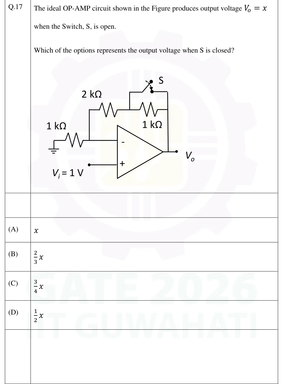
The ideal OP-AMP circuit shown in the Figure produces output voltage Vo=x when the Switch, S, is open.
Which of the options represents the output voltage when S is closed?
Tap to open full sizeFigure from the GATE 2026 EC paper. It is part of the question.Figure description
Non-inverting amplifier using an ideal op-amp. The non-inverting (+) input is driven by a source V_i = 1 V. The inverting (-) input node connects to ground through a 1 k Ω resistor. The feedback path from the inverting node to the output V_o is a 2 k Ω resistor in series with a 1 k Ω resistor (the 2 k Ω is on the inverting-node side, the 1 k Ω on the output side). A switch S is connected from the junction between the 2 k Ω and the 1 k Ω feedback resistors directly to the output line, i.e. S is in parallel with the 1 k Ω feedback resistor. S is drawn open. The output terminal is labelled V_o.
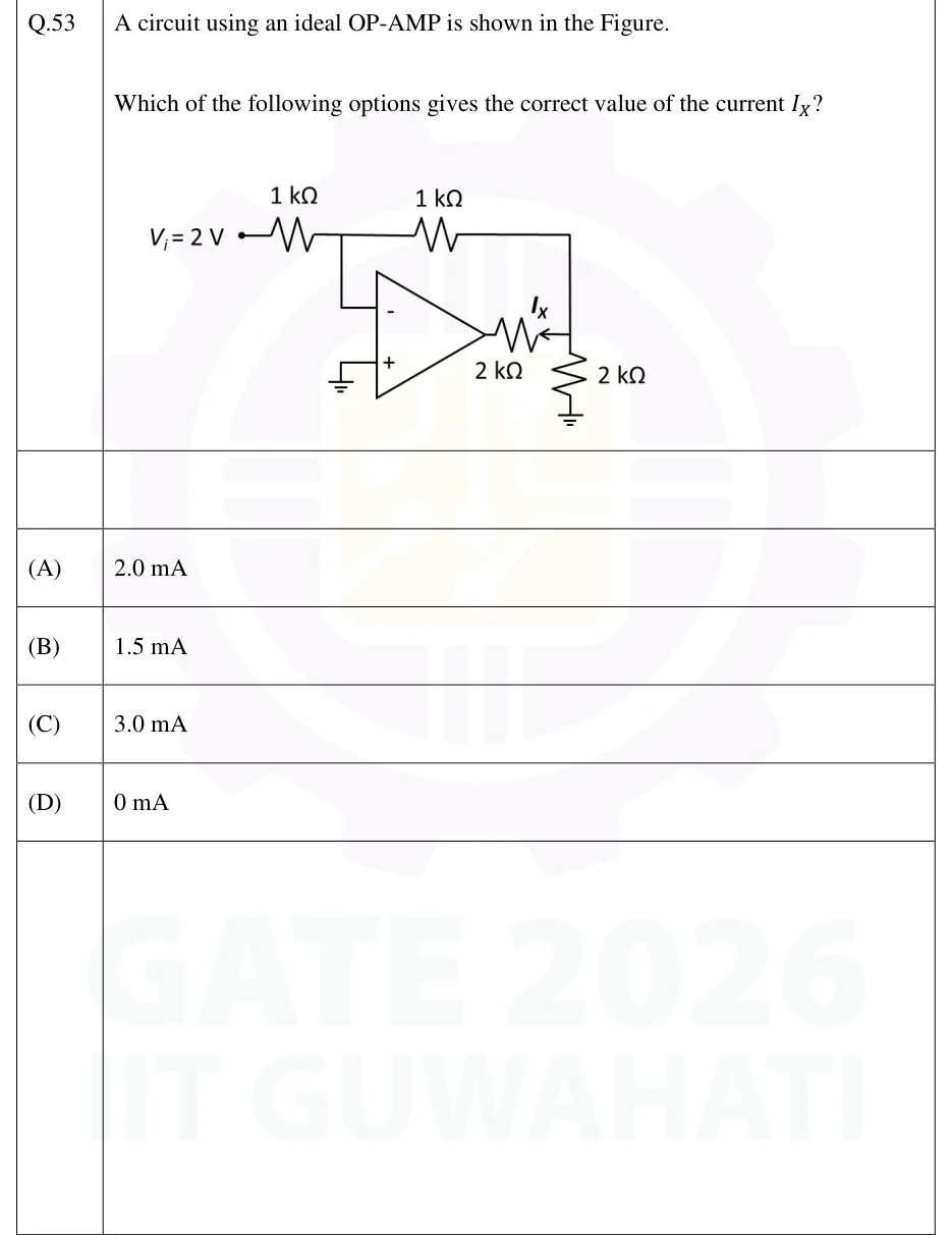
A circuit using an ideal OP-AMP is shown in the Figure.
Which of the following options gives the correct value of the current IX?
Tap to open full sizeFigure from the GATE 2026 EC paper. It is part of the question.Figure description
Ideal op-amp with its non-inverting (+) input grounded. Input source V_i = 2 V connects through a 1 k Ω resistor to the inverting (-) input node. A second 1 k Ω resistor runs from the inverting input node to a node on the right (call it X). The op-amp output connects to node X through a 2 k Ω resistor; the current I_X in this resistor is marked with an arrow pointing from node X toward the op-amp output. Node X is also connected to ground through another 2 k Ω resistor.
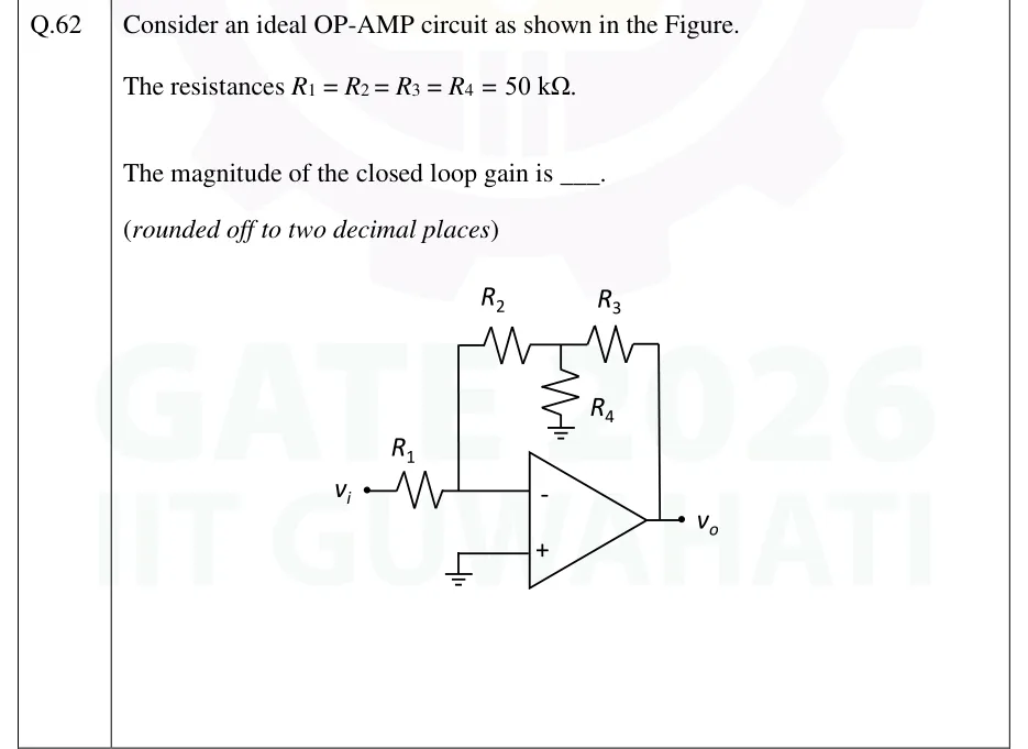
Consider an ideal OP-AMP circuit as shown in the Figure.
The resistances R1=R2=R3=R4=50kΩ.
The magnitude of the closed loop gain is ____.
(rounded off to two decimal places)
Tap to open full sizeFigure from the GATE 2026 EC paper. It is part of the question.Figure description
Inverting amplifier with a T-network in the feedback path. Input v_i connects through R_1 to the inverting (−) input of an ideal op-amp. The non-inverting (+) input is grounded. From the inverting input, R_2 goes up to an intermediate node X; from X, R_4 goes down to ground; from X, R_3 goes to the op-amp output v_o. So the feedback path is R_2 (inverting input to X), then R_3 (X to output), with R_4 shunting X to ground. R_1 = R_2 = R_3 = R_4 = 50 k Ω. No supply rails shown.
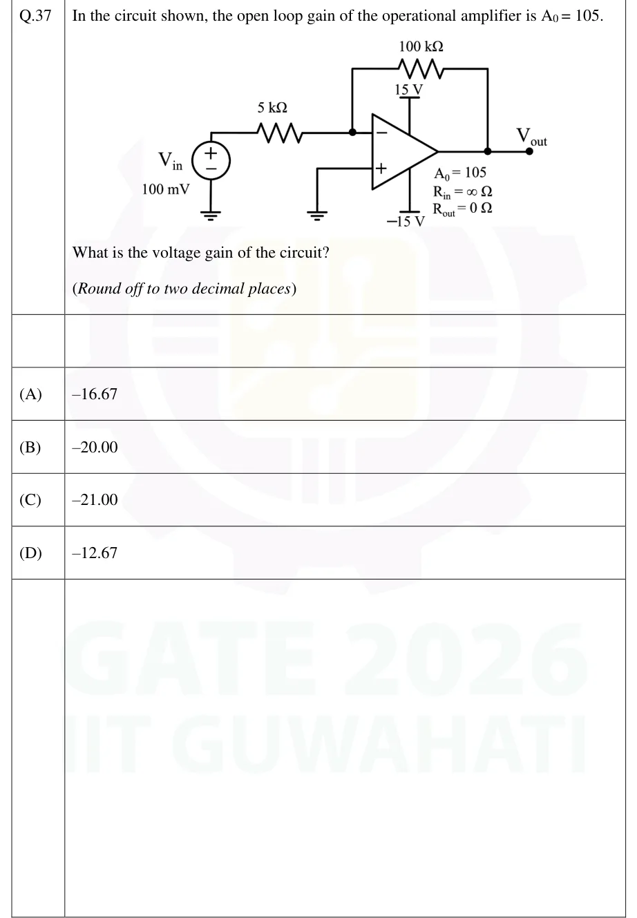
In the circuit shown, the open loop gain of the operational amplifier is A0=105.
What is the voltage gain of the circuit?
(Round off to two decimal places)
Tap to open full sizeFigure from the GATE 2026 EE paper. It is part of the question.Figure description
Inverting amplifier. An independent voltage source V_in = 100 mV has its + terminal at the top and its − terminal connected to ground. From the + terminal, a 5 kΩ resistor goes to the inverting (−) input of an op-amp. A 100 kΩ feedback resistor connects the inverting input to the op-amp output. The non-inverting (+) input is connected directly to ground. The op-amp's upper supply pin is labelled 15 V and its lower supply pin −15 V. The output node is labelled V_out. Printed beside the op-amp: A_0 = 105, R_in = ∞ Ω, R_out = 0 Ω.
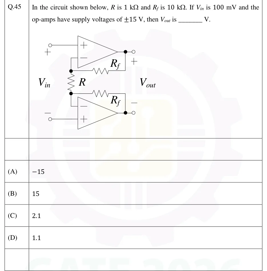
In the circuit shown below, R is 1kΩ and Rf is 10kΩ. If Vin is 100mV and the op-amps have supply voltages of ±15V, then Vout is ________ V.
Tap to open full sizeFigure from the GATE 2026 IN paper. It is part of the question.Figure description
Two op-amps, one above the other: the input stage of an instrumentation amplifier. Top op-amp: its non-inverting (+) input goes straight to the '+' terminal of the input V_in (upper left open terminal). Its inverting (−) input connects to a node at the top end of resistor R. A feedback resistor R_f runs from that node to the top op-amp's output, which is the upper output terminal, marked '+'. Resistor R runs vertically between the top node and a bottom node. Bottom op-amp: its inverting (−) input connects to the bottom node of R. A second feedback resistor R_f runs from the bottom node to the bottom op-amp's output, which is the lower output terminal, marked '−'. Its non-inverting (+) input goes straight to the '−' terminal of the input V_in (lower left open terminal). V_in is applied between the upper-left (+) and lower-left (−) terminals. V_out is taken between the two op-amp outputs (+ at the top output, − at the bottom output). Both op-amps run from ±15 V supplies.
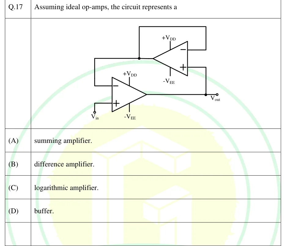
Tap to open full sizeFigure from the GATE 2025 EE paper. It is part of the question.Figure description
Two op-amps, each powered from +V_DD and -V_EE. Op-amp 1 (lower, pointing right): its non-inverting (+) input is driven by the input terminal V_in; its output is the circuit output node V_out. Op-amp 2 (upper, pointing left, so its output is on the left): its non-inverting (+) input (lower right) is wired to the V_out node; its inverting (−) input (upper right) is connected by a wire looping over the top back to its own output node on the left. That same output node of op-amp 2 is also wired down and left to the inverting (−) input of op-amp 1. The circuit has no resistors, capacitors or diodes.
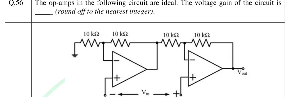
The op-amps in the following circuit are ideal. The voltage gain of the circuit is ______ (round off to the nearest integer).
Tap to open full sizeFigure from the GATE 2025 EE paper. It is part of the question.Figure description
Two ideal op-amps in cascade (a two-op-amp instrumentation/difference amplifier). Op-amp 1 (left): its inverting (−) input connects to the junction of two 10 kΩ resistors in series along the top; the left 10 kΩ goes from that junction to ground, the right 10 kΩ goes from that junction to the output of op-amp 1 (feedback). The non-inverting (+) input of op-amp 1 goes down to an open terminal marked '−' of the input voltage V_in. Op-amp 2 (right): the output of op-amp 1 connects through a 10 kΩ resistor to the junction at the inverting (−) input of op-amp 2, and a second 10 kΩ resistor goes from that junction to the output of op-amp 2 (feedback). The output of op-amp 2 is V_out. The non-inverting (+) input of op-amp 2 goes down to an open terminal marked '+' of V_in. V_in is drawn as a double-headed arrow between the '−' terminal (op-amp 1 + input) and the '+' terminal (op-amp 2 + input). All four resistors are 10 kΩ.
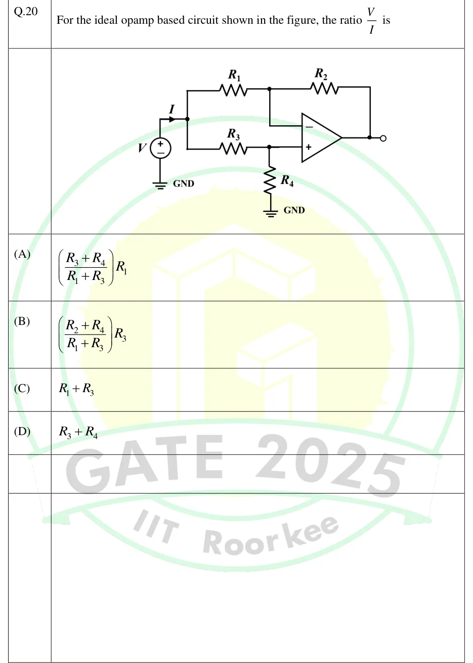
For the ideal opamp based circuit shown in the figure, the ratio IV is
Tap to open full sizeFigure from the GATE 2025 IN paper. It is part of the question.Figure description
An independent voltage source V (+ on top, − terminal to GND) drives a current I (arrow pointing right, out of the + terminal) into a node A. Two branches leave node A. Upper branch: resistor R_1 from A to a node N; node N connects to the inverting (−) input of an ideal op-amp, and resistor R_2 connects node N to the op-amp output (feedback path). Lower branch: resistor R_3 from A to a node P; node P connects to the non-inverting (+) input of the op-amp, and resistor R_4 connects node P to GND. The op-amp output goes to an open output terminal. No supply rails are drawn.
The circuits mentioned in the following options are realized using ideal opamp. Among these, the circuit(s) performing non-linear operation on the input signal is/are
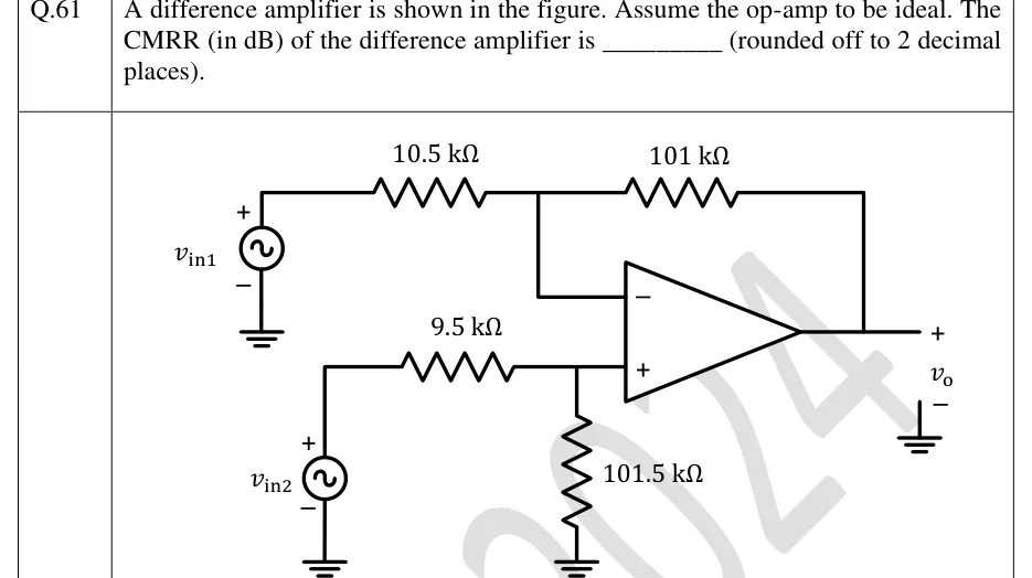
A difference amplifier is shown in the figure. Assume the op-amp to be ideal. The CMRR (in dB) of the difference amplifier is ________ (rounded off to 2 decimal places).
Tap to open full sizeFigure from the GATE 2024 EE paper. It is part of the question.Figure description
Single op-amp difference amplifier. Source v_in1 (+ terminal at top, − terminal to ground) connects through a 10.5 k Ω resistor to the op-amp's inverting (−) input. A 101 k Ω feedback resistor runs from the inverting input to the output v_o. Source v_in2 (+ at top, − to ground) connects through a 9.5 k Ω resistor to the non-inverting (+) input. A 101.5 k Ω resistor runs from the non-inverting input to ground. Output v_o is measured from the output node to ground (+ at the output).
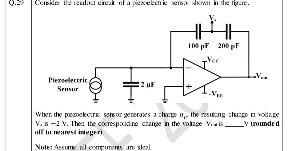
Consider the readout circuit of a piezoelectric sensor shown in the figure.
When the piezoelectric sensor generates a charge qp, the resulting change in voltage Vx is −2 V. Then the corresponding change in the voltage Vout is ______ V (rounded off to nearest integer).
Note: Assume all components are ideal.
Tap to open full sizeFigure from the GATE 2024 IN paper. It is part of the question.Figure description
A charge-amplifier readout circuit. On the left, the piezoelectric sensor is drawn as a current source (two overlapping circles) with its bottom terminal grounded and its top terminal on a horizontal wire. A 2 µF capacitor goes from that same wire to ground. The wire continues to the inverting (−) input of an op-amp. The op-amp's non-inverting (+) input is grounded. Its supplies are +V_CC (top) and −V_EE (bottom), and its output node is labelled V_out. The feedback path from the inverting input to V_out is two capacitors in series: 100 pF next to the inverting input, then 200 pF next to the output. The node between the two capacitors is brought out as terminal V_x.
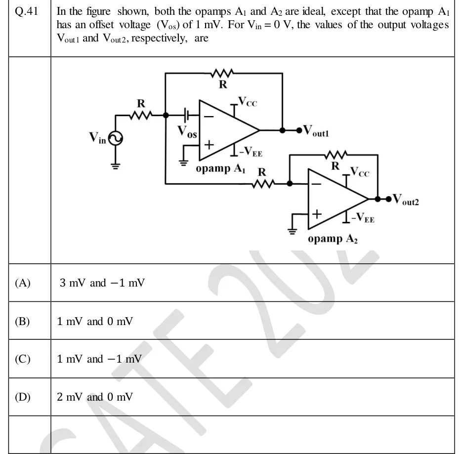
In the figure shown, both the opamps A1 and A2 are ideal, except that the opamp A1 has an offset voltage (Vos) of 1 mV. For Vin=0 V, the values of the output voltages Vout1 and Vout2, respectively, are
Tap to open full sizeFigure from the GATE 2024 IN paper. It is part of the question.Figure description
Two op-amps, A1 (upper) and A2 (lower), each powered by +V_CC and -V_EE. Source V_in (sinusoidal symbol, lower terminal grounded) feeds a resistor R into a node X. From node X: a feedback resistor R goes to V_out1 (output of A1); a battery V_os is in series between node X and the inverting (-) input of A1, drawn with its long plate (positive terminal) on the node X side and its short plate (negative terminal) on the op-amp's inverting input side; the non-inverting (+) input of A1 is grounded. Node X also connects, through another resistor R, to the inverting (-) input of A2; A2 has a feedback resistor R from its output V_out2 to its inverting input, and its non-inverting (+) input is grounded. All four resistors are equal to R.
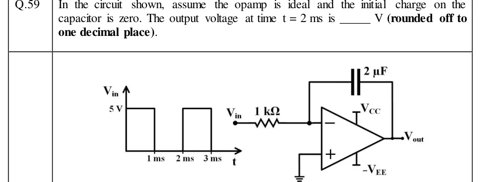
In the circuit shown, assume the opamp is ideal and the initial charge on the capacitor is zero. The output voltage at time t = 2 ms is ______ V (rounded off to one decimal place).
Tap to open full sizeFigure from the GATE 2024 IN paper. It is part of the question.Figure description
Left: a plot of V_in against t. V_in is a pulse train: 5 V from t = 0 to 1 ms, 0 V from 1 ms to 2 ms, 5 V again from 2 ms to 3 ms, then 0. Axis ticks are marked 1 ms, 2 ms, 3 ms, and the level is marked 5 V. Right: an inverting integrator. V_in goes through a 1 kΩ resistor to the inverting (−) input of the op-amp. A 2 µF capacitor connects the inverting input to the output V_out. The non-inverting (+) input is grounded. The op-amp is powered from supply rails V_CC and -V_EE, with no numerical values given.
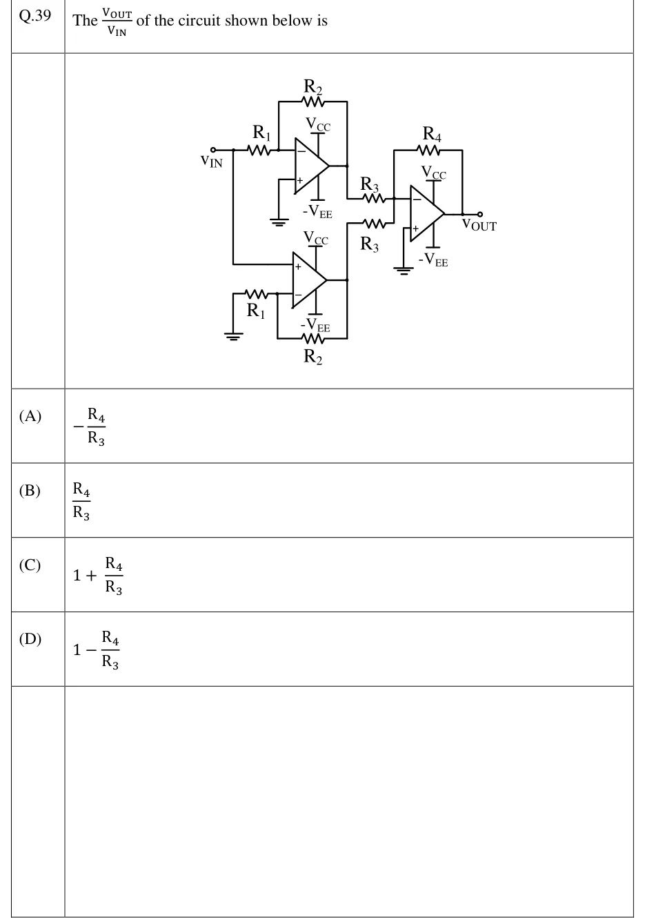
Tap to open full sizeFigure from the GATE 2023 EC paper. It is part of the question.Figure description
Three op-amps, each powered from V_CC (top rail) and -V_EE (bottom rail). Op-amp 1 (top left): V_IN is applied through R_1 to its inverting (−) input; R_2 is connected from its output back to the − input; its non-inverting (+) input is grounded. Op-amp 2 (bottom left): the V_IN node is also wired straight down to its non-inverting (+) input; its inverting (−) input goes to ground through R_1, and R_2 is connected from its output to the − input. Op-amp 3 (right): the output of op-amp 1 goes through a resistor R_3, and the output of op-amp 2 goes through a second resistor R_3. Both resistors join at the inverting (−) input of op-amp 3. R_4 is connected from the output of op-amp 3 back to its − input, and its + input is grounded. The output of op-amp 3 is V_OUT.
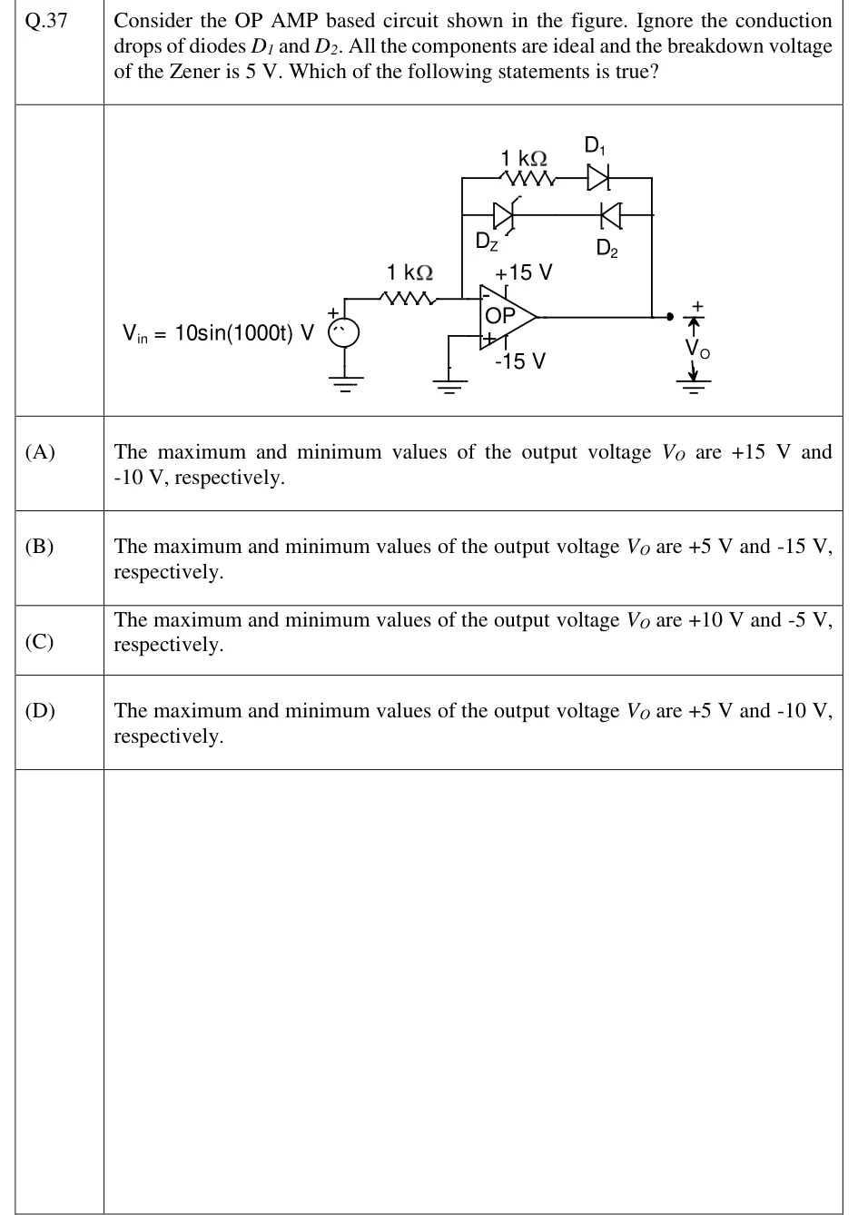
Consider the OP AMP based circuit shown in the figure. Ignore the conduction drops of diodes D1 and D2. All the components are ideal and the breakdown voltage of the Zener is 5 V. Which of the following statements is true?
Tap to open full sizeFigure from the GATE 2023 EE paper. It is part of the question.Figure description
Inverting op-amp circuit. Source V_in = 10 sin (1000t) V (+ terminal up, − terminal to ground) feeds a 1 kΩ resistor into the inverting (−) input of an op-amp labelled OP, powered from +15 V and −15 V rails. The non-inverting (+) input is grounded. The output node is labelled V_O (measured with respect to ground, + at the top). Between the inverting input and the output are two parallel feedback branches. Top branch: a 1 kΩ resistor in series with diode D_1, whose anode is on the inverting-input side and cathode on the output side. Lower branch: Zener diode D_Z in series with diode D_2; the Zener's anode is on the inverting-input side and its cathode faces D_2; D_2's cathode faces the Zener and its anode is on the output side (so the two diodes are cathode-to-cathode).
(A)
The maximum and minimum values of the output voltage VO are +15 V and -10 V, respectively.
(B)
The maximum and minimum values of the output voltage VO are +5 V and -15 V, respectively.
(C)
The maximum and minimum values of the output voltage VO are +10 V and -5 V, respectively.
(D)
The maximum and minimum values of the output voltage VO are +5 V and -10 V, respectively.
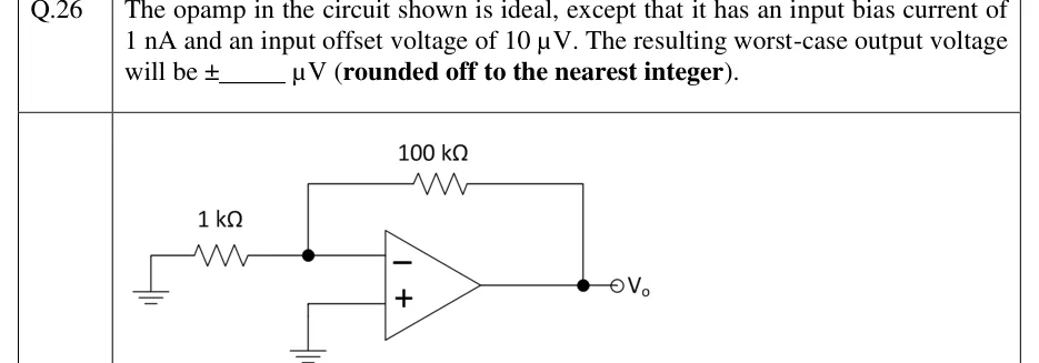
The opamp in the circuit shown is ideal, except that it has an input bias current of 1 nA and an input offset voltage of 10 μV. The resulting worst-case output voltage will be ± ______ μV (rounded off to the nearest integer).
Tap to open full sizeFigure from the GATE 2023 IN paper. It is part of the question.Figure description
Inverting-amplifier configuration with no input signal. A 1 kΩ resistor connects ground (left) to a node that goes to the op-amp's inverting (−) input. A 100 kΩ feedback resistor connects this inverting-input node to the op-amp output. The non-inverting (+) input is connected directly to ground (no resistor). The output node is labelled V_o.
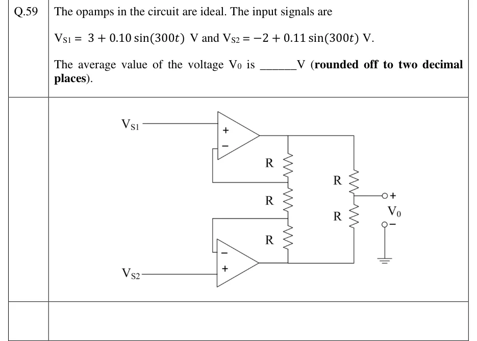
The opamps in the circuit are ideal. The input signals are
VS1=3+0.10sin(300t)V and VS2=−2+0.11sin(300t)V.
The average value of the voltage VO is ______ V (rounded off to two decimal places).
Tap to open full sizeFigure from the GATE 2023 IN paper. It is part of the question.Figure description
Two ideal op-amps, one above the other. Top op-amp: non-inverting (+) input is driven by V_S1; its inverting (−) input is wired to node A. Bottom op-amp: non-inverting (+) input is driven by V_S2; its inverting (−) input is wired to node B. Left resistor chain, three equal resistors R in series from the top op-amp's output down to the bottom op-amp's output: top op-amp output — R — node A — R — node B — R — bottom op-amp output. So each op-amp's feedback resistor is an outer R, and the middle R sits between the two inverting inputs. Right resistor chain: two equal resistors R in series from the top op-amp's output to the bottom op-amp's output. Their junction is the output terminal V_O (+). The V_O (−) terminal is ground. This is the input stage of the three-op-amp instrumentation amplifier, with its output taken at the midpoint of a two-resistor divider.
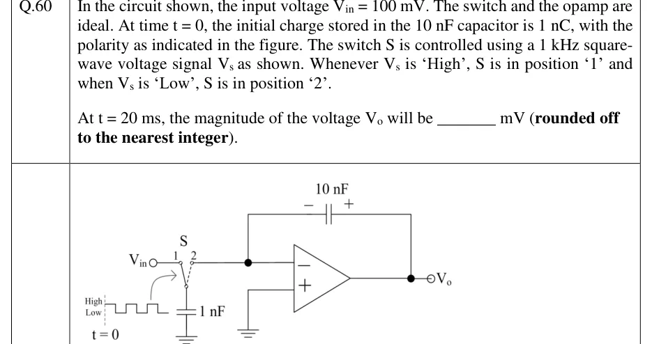
In the circuit shown, the input voltage Vin=100mV. The switch and the opamp are ideal. At time t=0, the initial charge stored in the 10nF capacitor is 1nC, with the polarity as indicated in the figure. The switch S is controlled using a 1kHz square-wave voltage signal Vs as shown. Whenever Vs is 'High', S is in position '1' and when Vs is 'Low', S is in position '2'.
At t=20ms, the magnitude of the voltage Vo will be ________ mV (rounded off to the nearest integer).
Tap to open full sizeFigure from the GATE 2023 IN paper. It is part of the question.Figure description
Switched-capacitor integrator. A single-pole double-throw switch S has its common (moving) terminal connected to the top plate of a 1 nF capacitor whose bottom plate is grounded. Throw '1' of S connects to the input terminal V_in; throw '2' connects to the inverting (−) input of an op-amp. A 10 nF capacitor is connected from the inverting input to the op-amp output V_o, with its polarity marked '−' on the inverting-input side (left plate) and '+' on the output side (right plate). The non-inverting (+) input of the op-amp is grounded. No other components. A curved arrow from the control waveform to the switch indicates V_s drives S. Control waveform V_s: a square wave between levels 'Low' and 'High', starting at t = 0 (dashed vertical line) in the High state, then Low, High, Low, High, Low (equal half-periods); frequency 1 kHz.
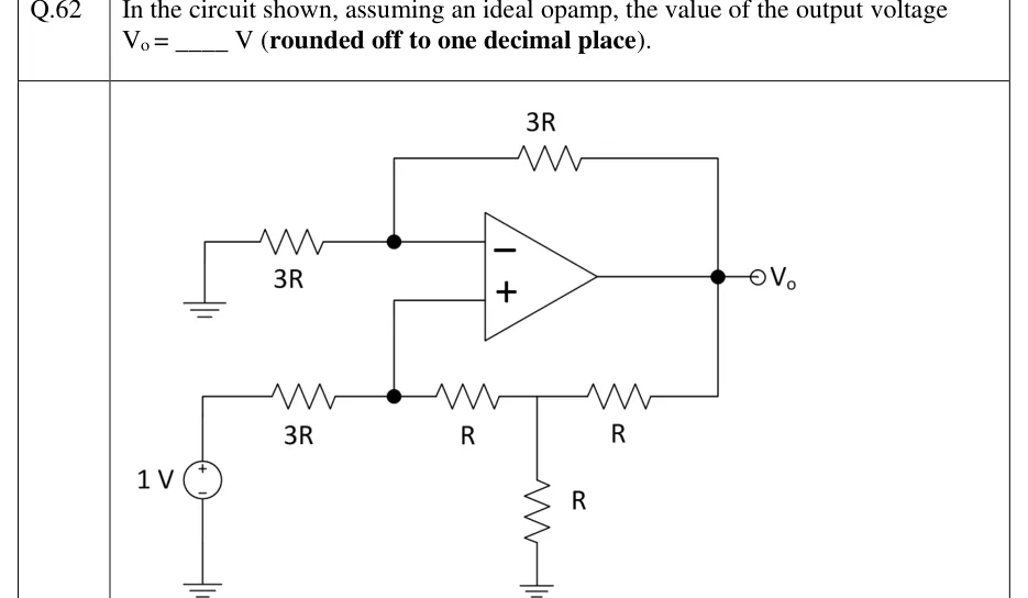
In the circuit shown, assuming an ideal opamp, the value of the output voltage Vo = ____ V (rounded off to one decimal place).
Tap to open full sizeFigure from the GATE 2023 IN paper. It is part of the question.Figure description
Op-amp with inverting (−) input on top and non-inverting (+) input below; output node labelled V_o on the right. Inverting-input node: a 3R resistor from ground to this node, and a 3R feedback resistor from this node to V_o. Non-inverting-input node (call it P): a 3R resistor from the positive terminal of a 1 V DC source (negative terminal grounded) to P; a resistor R from P to a second node X; node X has a resistor R to ground and a resistor R to the output V_o.
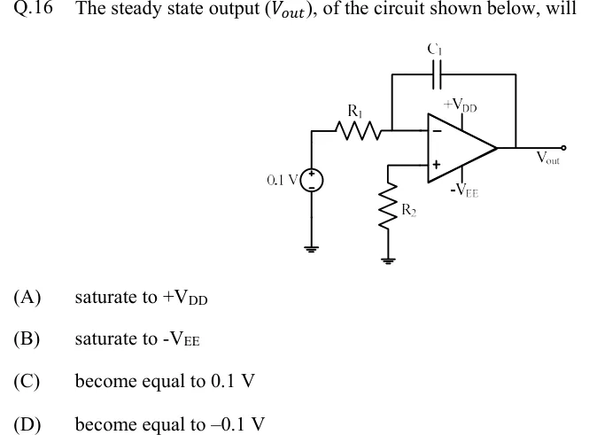
The steady state output (Vout), of the circuit shown below, will
Tap to open full sizeFigure from the GATE 2022 EE paper. It is part of the question.Figure description
Op-amp circuit powered from +V_DD (top) and -V_EE (bottom). A 0.1 V DC source (+ terminal on top, - terminal to ground) drives resistor R1, whose other end connects to the inverting (-) input of the op-amp. Capacitor C1 is connected from the inverting input to the output (feedback path); there is no resistor across C1. The non-inverting (+) input goes to ground through resistor R2. The output node is labelled V_out. No component values are given other than the 0.1 V source.
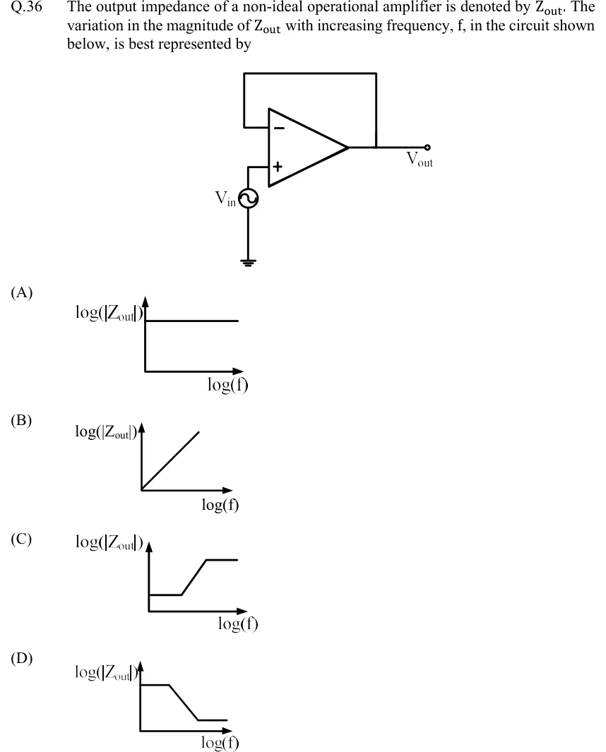
The output impedance of a non-ideal operational amplifier is denoted by Zout. The variation in the magnitude of Zout with increasing frequency, f, in the circuit shown below, is best represented by
Tap to open full sizeFigure from the GATE 2022 EE paper. It is part of the question.Figure description
Op-amp voltage follower (unity-gain buffer). The op-amp output is connected directly by a wire back to its inverting (−) input; there are no resistors. The non-inverting (+) input is driven by an AC source V_in whose other terminal is grounded. The output node is labelled V_out. Options are four plots of log (|Z_out|) (vertical axis) against log (f) (horizontal axis).
(A)
Figure — log(∣Zout∣) vs log(f): a horizontal line, constant at all frequencies.
(B)
Figure — log(∣Zout∣) vs log(f): a straight line rising from the origin, increasing at all frequencies.
(C)
Figure — log(∣Zout∣) vs log(f): flat at a low level, then a rising straight segment, then flat again at a higher level.
(D)
Figure — log(∣Zout∣) vs log(f): flat at a high level, then a falling straight segment, then flat again at a lower level.
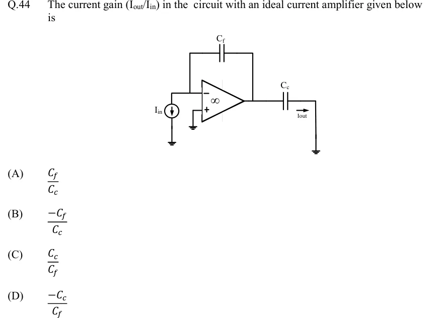
Q.44 The current gain (Iout/Iin) in the circuit with an ideal current amplifier given below is
Tap to open full sizeFigure from the GATE 2022 EE paper. It is part of the question.Figure description
An ideal op-amp (gain marked ∞). Its non-inverting (+) input is grounded. A capacitor C_f is connected from the op-amp output back to the inverting (−) input. An independent current source I_in is connected between the inverting (−) input node and ground; its arrow points downward, so it draws current I_in out of the inverting node into ground. The op-amp output is connected through a series capacitor C_c to ground; the current through C_c, flowing from the output towards ground, is labelled I_out (arrow pointing right, away from the op-amp).
An OPAMP has a gain of 104, an input impedance of 10MΩ and an output impedance of 100Ω. The OPAMP is used in unity-gain feedback configuration in a voltage buffer circuit. The closed-loop output impedance of the OPAMP (in milliohms) in the circuit is ________ (round off to one decimal place)
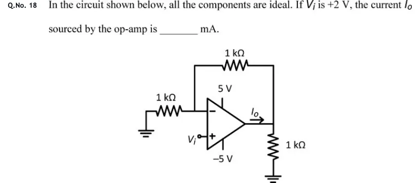
In the circuit shown below, all the components are ideal. If Vi is +2V, the current Io sourced by the op-amp is ________ mA.
Tap to open full sizeFigure from the GATE 2020 EC paper. It is part of the question.Figure description
Non-inverting op-amp amplifier. The op-amp is powered from +5 V (top rail) and -5 V (bottom rail). The input V_i is applied directly to the non-inverting (+) input. The inverting (-) input is connected to ground through a 1 kΩ resistor, and to the op-amp output through a 1 kΩ feedback resistor. The output node is connected to ground through a 1 kΩ load resistor. An arrow labelled I_o points out of the op-amp output terminal toward the output node, before it splits between the feedback resistor and the load resistor.
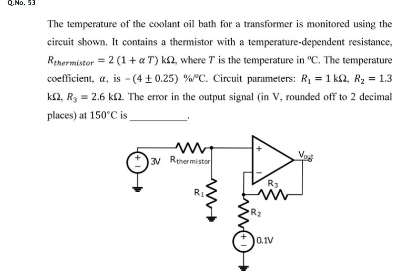
The temperature of the coolant oil bath for a transformer is monitored using the circuit shown. It contains a thermistor with a temperature-dependent resistance, Rthermistor=2(1+αT)kΩ, where T is the temperature in ∘C. The temperature coefficient, α, is −(4±0.25)%/∘C. Circuit parameters: R1=1kΩ,R2=1.3kΩ,R3=2.6kΩ. The error in the output signal (in V, rounded off to 2 decimal places) at 150∘C is ________.
Tap to open full sizeFigure from the GATE 2020 EE paper. It is part of the question.Figure description
Op-amp circuit. On the left, a 3 V DC source with + terminal at the top and - terminal grounded. From the + terminal, a resistor labelled R_thermistor runs right to a node that connects to the non-inverting (+) input of the op-amp; a resistor R1 goes from that same node down to ground (so R_thermistor and R1 form a divider of the 3 V source feeding the + input). The inverting (-) input connects to a node from which R3 runs to the output V_out (feedback resistor), and R2 runs down to the + terminal of a 0.1 V DC source whose - terminal is grounded. The op-amp output is labelled V_out.
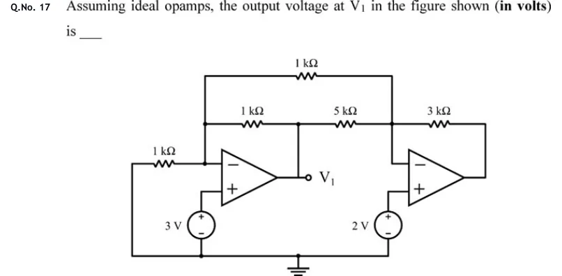
Assuming ideal opamps, the output voltage at V1 in the figure shown (in volts) is ____
Tap to open full sizeFigure from the GATE 2020 IN paper. It is part of the question.Figure description
Two op-amps. LEFT op-amp: inverting input (−) on top, non-inverting input (+) below; its output is the node labelled V1. The (+) input goes to the positive terminal of a 3 V source whose negative terminal is on the bottom ground rail. The (−) input connects to node A. Node A has three branches: (i) a 1 kΩ resistor going left, whose far end drops down to the bottom ground rail; (ii) a 1 kΩ resistor (middle row) going right to the V1 node (V1 connects up to this row); (iii) a 1 kΩ resistor along the top row going right to node B. From the V1 node, a 5 kΩ resistor (middle row) also goes right to node B. RIGHT op-amp: inverting input (−) on top, non-inverting input (+) below. Its (−) input is node B; its (+) input goes to the positive terminal of a 2 V source whose negative terminal is on the ground rail. Its output loops back up and through a 3 kΩ resistor to node B. The bottom rail carries the ground symbol and ties together the far end of the left 1 kΩ and the negative terminals of both sources.
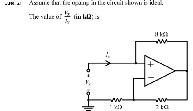
Assume that the opamp in the circuit shown is ideal.
The value of IxVx (in kΩ) is ____
Tap to open full sizeFigure from the GATE 2020 IN paper. It is part of the question.Figure description
An op-amp with its non-inverting (+) input on top and its inverting (−) input below; output on the right. A test source terminal pair on the left: the upper terminal is marked +, the lower terminal is marked − and is grounded, and the voltage between them is V_x. A current I_x flows from the upper terminal (arrow pointing right) into a node connected directly to the non-inverting (+) input. From that same node, an 8 kΩ resistor goes up and across to the op-amp output (positive feedback path). The inverting (−) input is wired down to a node on the bottom line. On the bottom line, a 1 kΩ resistor connects the grounded lower terminal to that node, and a 2 kΩ resistor connects that node to the op-amp output. So the inverting input sits at the junction of a 2 kΩ (to output) and 1 kΩ (to ground) divider, and the 8 kΩ resistor links the input node (at V_x) to the output.
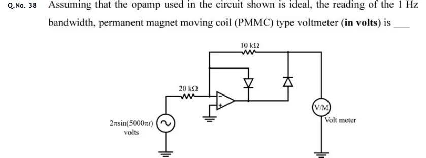
Assuming that the opamp used in the circuit shown is ideal, the reading of the 1 Hz bandwidth, permanent magnet moving coil (PMMC) type voltmeter (in volts) is ____
Tap to open full sizeFigure from the GATE 2020 IN paper. It is part of the question.Figure description
Inverting precision half-wave rectifier. A source 2 π sin (5000 π t) volts, with its lower terminal grounded, feeds a 20 kΩ resistor into the inverting (−) input of an op-amp. The non-inverting (+) input is grounded. The inverting-input node runs up to a top rail, and a 10 kΩ resistor on that rail connects it to the right-hand output node. Diode D1 connects the inverting-input node (anode, top) to the op-amp output (cathode, bottom). Diode D2 connects the op-amp output (anode, bottom) to the right-hand output node (cathode, top). A voltmeter (V/M, labelled 'Volt meter') is connected from the right-hand output node to ground.
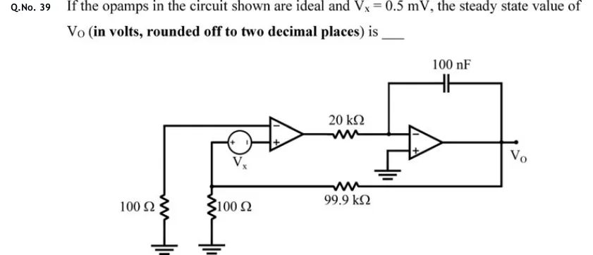
If the opamps in the circuit shown are ideal and VX=0.5mV, the steady state value of VO (in volts, rounded off to two decimal places) is ____
Tap to open full sizeFigure from the GATE 2020 IN paper. It is part of the question.Figure description
Two ideal op-amps in cascade. Op-amp 1 (left): its inverting (−, upper) input is connected by a wire to the top of a 100 Ω resistor whose other end is grounded (far left). Its non-inverting (+, lower) input is connected to the '−' terminal of a DC source V_X; the '+' terminal of V_X (left side) goes to a node N. Node N is the top of a second 100 Ω resistor to ground, and is also connected through a 99.9 kΩ resistor to the output V_O. Output of op-amp 1 goes through a 20 kΩ resistor to the inverting (−) input of op-amp 2 (right); op-amp 2's non-inverting (+) input is grounded; a 100 nF capacitor connects op-amp 2's inverting input to its output. The output of op-amp 2 is V_O, which feeds back to node N through the 99.9 kΩ resistor. So op-amp 2 is an inverting integrator (R = 20 kΩ, C = 100 nF) and the loop is closed from V_O through the 99.9 kΩ / 100 Ω divider and V_X back to op-amp 1's + input.
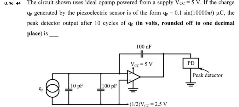
The circuit shown uses ideal opamp powered from a supply VCC=5 V. If the charge qp generated by the piezoelectric sensor is of the form qp=0.1sin(10000πt)μC, the peak detector output after 10 cycles of qp (in volts, rounded off to one decimal place) is ____
Tap to open full sizeFigure from the GATE 2020 IN paper. It is part of the question.Figure description
Charge-amplifier circuit. On the left is the piezoelectric sensor, drawn as a current source (two overlapping circles, no arrow) labelled q_p. Two capacitors, 10 pF and 100 pF, are connected in parallel with it between a top rail and a bottom rail. The top rail goes to the inverting (-) input of the op-amp. The bottom rail (the sensor's lower terminal and the lower plates of both capacitors) runs right to a terminal labelled (1/2)V_CC = 2.5 V. The non-inverting (+) input is wired to this same bottom rail, so it sits at 2.5 V. A 100 nF capacitor connects the op-amp output back to the inverting input. The op-amp's positive supply pin is marked V_CC = 5 V and its negative supply pin goes to ground (single supply). The op-amp output feeds a block labelled PD (Peak detector), which has a ground connection below it. The PD output is the quantity asked for.
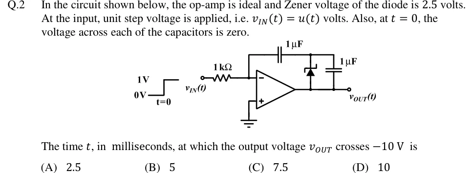
In the circuit shown below, the op-amp is ideal and Zener voltage of the diode is 2.5 volts. At the input, unit step voltage is applied, i.e. vIN(t)=u(t) volts. Also, at t=0, the voltage across each of the capacitors is zero.
The time t, in milliseconds, at which the output voltage vOUT crosses −10V is
Tap to open full sizeFigure from the GATE 2018 EC paper. It is part of the question.Figure description
Inverting integrator-type circuit with an ideal op-amp. Input: a unit step waveform (0 V before t = 0, 1 V after t = 0) is applied as v_IN(t) through a 1 kΩ resistor to the inverting (−) input. The non-inverting (+) input is grounded. Feedback network from the inverting input node to the op-amp output: a 1 µF capacitor (C1) connected along the top wire from the inverting-input node to a node X; from node X down to the output line there are two elements in parallel: a Zener diode (cathode at node X on top, anode at the output line below, triangle pointing up) and a second 1 µF capacitor (C2). So the feedback is C1 in series with (Zener || C2). The output line continues to the right as v_OUT(t). Both capacitors are uncharged at t = 0; Zener voltage 2.5 V.
Q.38 An op-amp based circuit is implemented as shown below.
[Figure]
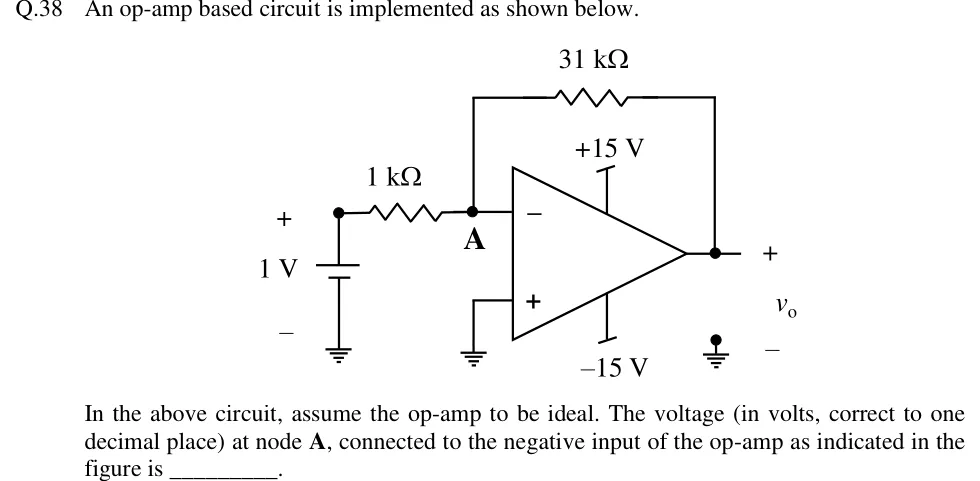
In the above circuit, assume the op-amp to be ideal. The voltage (in volts, correct to one decimal place) at node A, connected to the negative input of the op-amp as indicated in the figure is ________.
Tap to open full sizeFigure from the GATE 2018 EC paper. It is part of the question.Figure description
An inverting amplifier. A 1 V DC source (battery, + terminal on top, − terminal to ground) connects through a 1 kΩ resistor to node A. Node A is the op-amp's inverting (−) input. A 31 kΩ feedback resistor connects node A to the op-amp output. The non-inverting (+) input is grounded. The op-amp is powered from +15 V (top rail) and −15 V (bottom rail). The output node is labelled v_o (+ at the output, − at ground).
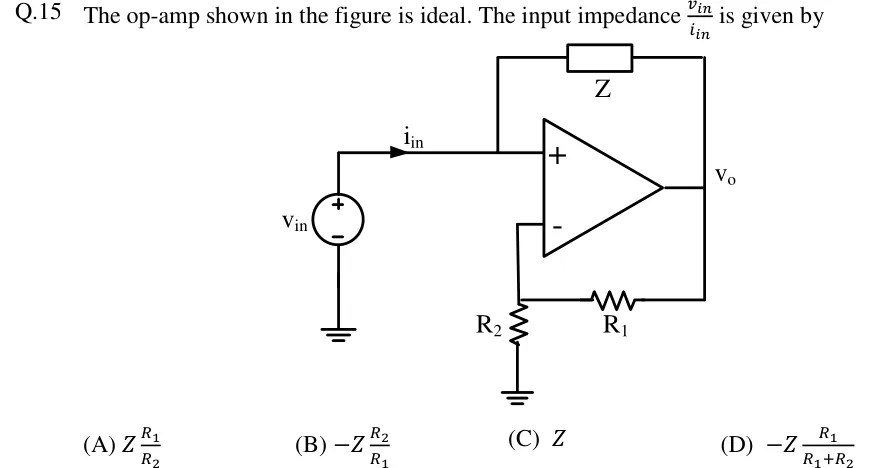
The op-amp shown in the figure is ideal. The input impedance iinvin is given by
Tap to open full sizeFigure from the GATE 2018 EE paper. It is part of the question.Figure description
An ideal op-amp with its non-inverting (+) input at the top and its inverting (-) input at the bottom; output node labelled V_o on the right. A voltage source v_in (+ terminal up, - terminal to ground) drives a current i_in (arrow pointing right, toward the op-amp) into the node at the non-inverting (+) input. An impedance Z connects this non-inverting input node to the output V_o (drawn above the op-amp). The inverting (-) input goes to a node that is grounded through resistor R_2 and connected to the output V_o through resistor R_1 (drawn below the op-amp). So R_1 and R_2 form a divider from V_o to ground, with the tap at the inverting input.
An opamp that is powered from a ±5 V supply is used to build a non-inverting amplifier having a gain of 15. The slew rate of the opamp is 0.5×10⁶ V/s. For a sinusoidal input with amplitude of 0.3 V, the maximum frequency (in kHz) up to which it can be operated without any distortion is (up to one decimal place) ____.
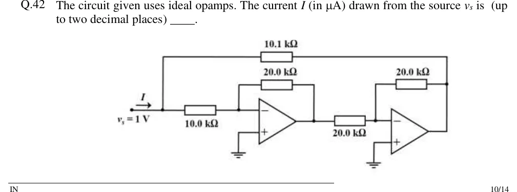
The circuit given uses ideal opamps. The current I (in μA) drawn from the source vs is (up to two decimal places) ____.
Tap to open full sizeFigure from the GATE 2018 IN paper. It is part of the question.Figure description
A source v_s = 1 V drives a node; the current I flows from the source into that node (arrow pointing right). From this node, a 10.0 k Ω resistor goes to the inverting (−) input of op-amp 1, and a 10.1 k Ω resistor runs along the top of the drawing to the output of op-amp 2. Op-amp 1: non-inverting (+) input grounded, 20.0 k Ω feedback resistor from its output to its inverting input. The output of op-amp 1 feeds a 20.0 k Ω resistor into the inverting (−) input of op-amp 2. Op-amp 2: non-inverting (+) input grounded, 20.0 k Ω feedback resistor from its output to its inverting input. The output of op-amp 2 is also the right-hand end of the 10.1 k Ω resistor that goes back to the source node.
An inverting amplifier with R1=2kΩ and Rf=18kΩ uses an op-amp with a single-pole open-loop response, DC gain 105 and unity-gain frequency ft=1 MHz. The closed-loop 3-dB bandwidth, in kHz, is ______.
▸ Answer and solution
Answer:100 (accepted range ±0.5)
Feedback factor: β=R1+RfR1=202=0.1. The noise gain is 10, even though the signal gain is −9.
fb=ft/A0=10 Hz, so f3dB=fb(1+A0β)=10×10001≈100 kHz, which equals βft.
Dividing by the signal gain instead (1 MHz / 9 = 111 kHz) is the trap: the bandwidth of an inverting amplifier is ft divided by 1+Rf/R1.
PRACTICE 22 marks · NAT
A difference amplifier uses an ideal op-amp. v1 is applied through R1=10kΩ to the inverting input, with R2=100kΩ from the output to the inverting input. v2 is applied through R3=10kΩ to the non-inverting input, with R4=101kΩ from the non-inverting input to ground. Taking vd=v2−v1 and vcm=(v1+v2)/2, the CMRR of the circuit, in dB, is ______ (to one decimal place).
▸ Answer and solution
Answer:60.9 (accepted range ±0.1)
By superposition, vo=−R1R2v1+Kv2 with K=R1(R3+R4)(R1+R2)R4=10×111110×101=10.009009.
Substituting v1=vcm−vd/2 and v2=vcm+vd/2 gives Ad=21(10+K)=10.004505 and Acm=K−10=0.009009=1/111.
CMRR=Ad/Acm=10.004505×111=1110.5.
20log10(1110.5)=60.9 dB. A 1% error in a single resistor limits the CMRR to about 61 dB even with a perfect op-amp.
PRACTICE 31 mark · MCQ
For which of the following circuits, built with an ideal op-amp and operating normally, is it NOT valid to assume v+=v−?
(A)
Voltage follower
(B)
Inverting integrator with a resistor Rf across the capacitor
(C)
Inverting Schmitt trigger (output fed back to v+ through a resistive divider, input applied at v−)
(D)
Three-op-amp instrumentation amplifier
▸ Answer and solution
Answer: (C)
The virtual short needs net negative feedback with the output inside its linear range.
A, B and D feed the output back to the inverting input, so v−=v+ holds.
The Schmitt trigger feeds back to v+ (positive feedback). Its output latches at ±Vsat, and v+=v− except at the switching instant.
PRACTICE 41 mark · NAT
A three-op-amp instrumentation amplifier uses ideal op-amps. In the first stage, each op-amp has R=25kΩ from its output to its inverting input, and RG=1kΩ joins the two inverting inputs. The difference stage is balanced, with input resistors R3=10kΩ and feedback and ground resistors R4=20kΩ. The inputs are v1=2.000 V and v2=2.010 V, and v2 drives the op-amp whose output feeds the non-inverting side of the difference stage. The output voltage, in volts, is ______.
▸ Answer and solution
Answer:1.02 (accepted range ±0.005)
The virtual shorts put v2−v1=10 mV across RG, so a current of 10mV/1kΩ=10μA flows through R,RG and R in series.
vo2=v2+R(10μA)=2.010+0.25=2.26 V and vo1=v1−0.25=1.75 V, so vo2−vo1=0.51 V =(1+2R/RG)(10mV)=51×10 mV. The 2 V common-mode level appears at both outputs and cancels.
Difference stage: vo=R3R4(vo2−vo1)=2×0.51=1.02 V.
PRACTICE 52 marks · MSQ
A non-inverting amplifier has R1=1kΩ (from v− to ground) and Rf=99kΩ. The op-amp is ideal except for an input offset voltage of magnitude 1 mV and input bias currents IB1=105 nA into the inverting input and IB2=95 nA into the non-inverting input. The signal source is an ideal voltage source (zero resistance) set to zero. Which of the following statements is/are correct?
(A)
The output error due to the offset voltage alone has magnitude 100 mV.
(B)
With the source connected directly to v+, the output error due to the bias currents alone is 10.395 mV.
(C)
Inserting a 990 Ω resistor in series with the non-inverting input reduces the output error due to the bias currents to 0.99 mV.
(D)
The 990 Ω resistor in option C also reduces the output error caused by the offset voltage.
▸ Answer and solution
Answer: (A), (B), (C)
VOS is multiplied by the noise gain: 1mV×(1+99/1)=100 mV. A is correct.
With v+=0,v−=0, so no current flows in R1 and all of IB1 flows through Rf:Vo=IB1Rf=105nA×99kΩ=10.395 mV. B is correct.
R1∥Rf=1001×99kΩ=990Ω. With it, v+=−IB2(990Ω) and Vo=Rf(IB1−IB2)=99kΩ×10nA=0.99 mV. C is correct.
The resistor balances only the bias currents. The offset-voltage term is still VOS(1+Rf/R1)=100 mV, so D is wrong.
PRACTICE 62 marks · NAT
An op-amp connected as a voltage follower (β=1) has loop gain L(jf)=(1+jf/10)(1+jf/(2×106))105, with f in Hz. Using the exact gain-crossover frequency (not the straight-line approximation), the phase margin, in degrees, is ______ (to one decimal place).
▸ Answer and solution
Answer:65.5 (accepted range ±0.2)
Well above 10 Hz, ∣L∣≈f1+(f/f2)2105×10=f1+(f/f2)2106 with f2=2 MHz.
Let x=fc/f2. Setting ∣L∣=1 gives 2×106x1+x2106=1, so 4x4+4x2−1=0 and x2=22−1=0.2071. Hence x=0.4551 and fc=910 kHz.
Phase at crossover: ∠L=−tan−1(fc/10)−tan−1(0.4551)=−89.999∘−24.47∘=−114.47∘.
PM=180∘−114.47∘=65.5∘. The straight-line estimate (crossover at 1 MHz) would give 63.4∘.
Cross-check: here βft=1 MHz =f2/2, so ζ=212=0.707, the maximally flat two-pole case, whose phase margin is 65.5∘.

 Tap to open full size