IAE Academy

GATE EC · EE · IN

Small-signal amplifiers

Small-signal amplifiers, frequency response, current mirrors and differential amplifiers

Small-signal analysis replaces each transistor by a linear model around its DC operating point: , and for a BJT, and for a MOSFET. With that model, the voltage gain, input resistance and output resistance of CE/CS, CB/CG, CC/CD, cascode and differential stages all follow from a few resistance-reflection rules. Frequency response brings in the capacitors. Coupling and bypass capacitors set the low-frequency cut-off, and device capacitances, magnified by the Miller effect, set the high-frequency cut-off. Current mirrors bias and load these stages, and a differential pair with a current-source tail is the usual input stage of an op-amp. Every convention is stated up front, and every result is given with the conditions under which it holds.

20 previous-year questions · 20 solved · 5 practice questions

Conventions and small-signal models

Conventions used throughout. is the thermal voltage, taken as 25 mV at room temperature. Use 26 mV if a question says so; answers then change by about 4%. The MOSFET threshold voltage is written so that it does not clash with . BJT: hybrid-π model with and . The base spreading resistance is neglected, and is neglected unless a value is given. means the small-signal , taken equal to the DC value. NMOS in saturation follows the square law , with overdrive and (no ) unless given. Body effect is neglected unless , or is given. Parallel resistors: .

The small-signal procedure. (1) Do the DC analysis first: find (or ) and confirm the active region (saturation for a MOSFET). (2) Compute the model parameters from that bias. (3) Draw the AC equivalent circuit. DC voltage sources become AC ground and ideal DC current sources become open circuits. At midband, coupling and bypass capacitors are short circuits and device capacitances are open circuits. (4) Replace each transistor by its model and solve the linear circuit.

AC coupling is what makes this separation possible. A coupling capacitor passes the signal but blocks DC, so the source and the load do not disturb the bias point. The linear model holds only for small signals: for a BJT and for a MOSFET.

BJT HYBRID-Π PARAMETERS

Active region, DC collector current , Early voltage . is the resistance looking into the emitter with the base at AC ground (T-model), and . Example: at mA with mV, mA/V.

MOSFET SMALL-SIGNAL PARAMETERS

NMOS in saturation, square law. The expression uses . The gate draws no current, so the resistance looking into the gate is infinite. The body-effect transconductance matters only when a signal appears between source and body, as in CG and CD stages with the body tied to a rail. Its value depends on the DC source-body voltage through . Neglect it unless the question gives , or .

INTRINSIC GAIN (THE MOST ONE TRANSISTOR CAN GIVE)

This is the magnitude of the gain of a CE/CS stage loaded only by its own , as with an ideal current-source load. For a BJT it does not depend on the bias current.

H-PARAMETER (CE) EQUIVALENTS OF THE HYBRID-Π MODEL

Low-frequency CE h-parameters, defined by and . , the reverse voltage feedback, is very small and is dropped in the approximate model.

TWO-PORT AMPLIFIER ANALYSIS WITH H-PARAMETERS (ANY CONFIGURATION)

enters the input terminal, enters the output terminal, and flows into the load . is the source resistance. is the admittance looking back into the output terminals with the source set to zero. The gain from the source is . Use the h-parameters of the configuration in use (CE, CB or CC). The approximate CE result, with and , is , and .

CB AND CC H-PARAMETERS FROM CE VALUES

The CB values are approximate, with small terms in and neglected. The CC values are exact conversions, except that is dropped from . is the same quantity as .

Quantity

BJT (active)

MOSFET (saturation)

Transconductance

: linear in , independent of device size

Resistance at the control terminal

(finite)

Infinite (gate)

Resistance looking into emitter / source (base / gate at AC ground)

, or with body effect

Diode-connected (collector–base or drain–gate shorted)

; with body effect

Output resistance

Intrinsic gain

(independent of bias)

EXAM TIP

How scales with bias. BJT: doubling doubles and halves both and . MOSFET with fixed : doubling multiplies by , multiplies by and halves , so falls by a factor of . Use only with the that belongs to that .

EXAM TIP

Symbol trap. In a mixed BJT/MOSFET question, can mean either the thermal voltage (about 25 mV) or the MOSFET threshold (typically hundreds of mV). Read the given values before substituting.

Single-transistor stages: gain, input and output resistance

Almost every midband result follows from a few resistance-reflection rules plus Ohm's law at the output. For a quick check of a CE/CS voltage gain from base (gate) to collector (drain), with and neglected: gain magnitude ≈ (total AC resistance at the collector or drain) ÷ (total resistance in the emitter or source path, including or ).

RESISTANCE-REFLECTION RULES (BJT)

is the total AC resistance from emitter to ground. is the total AC resistance from base to ground, i.e. the Thevenin resistance driving the base. neglected. An impedance in the emitter looks times larger from the base, and an impedance in the base looks times smaller from the emitter.

RESISTANCE RULES (MOSFET)

Gate at AC ground, neglected. No gate current flows, so any resistance in series with the gate carries no signal current. Including and a drain load gives .

CE / CS VOLTAGE GAIN, WITH OR WITHOUT DEGENERATION

() is the unbypassed emitter (source) resistance, and is the total AC load at the collector (drain). and body effect neglected. With the emitter fully bypassed () this reduces to . The approximation holds when (), which makes the gain almost independent of and temperature. The minus sign is a 180° phase inversion.

OVERALL GAIN FROM THE SIGNAL SOURCE

includes the bias network, e.g. . is the loaded gain from the transistor's input terminal to the output.

Notation for the table. (or ) is the total AC load at the collector or drain. For followers, and . is the bias divider and . Gains run from the transistor's input terminal to the output: is the base, emitter, gate or source voltage. Multiply by to get the gain from the source. is neglected. The CB and CG rows assume the base (gate) is at AC ground, i.e. any base bias resistors are bypassed. For a CE or CS stage whose emitter or source is at AC ground, including just adds to and to .

Stage

Voltage gain

Input resistance

Output resistance

Character

CE, emitter bypassed

()

Inverting; high voltage and current gain

CE, unbypassed

Inverting; lower but stable gain, higher

CB (input at emitter)

Non-inverting; current gain , very low

CC (emitter follower)

Voltage buffer; gain just below 1, current gain

CS, source bypassed

()

Inverting

CS, unbypassed

Inverting; degenerated

CG (input at source)

Non-inverting; current buffer

CD (source follower)

Voltage buffer; gain below 1

OUTPUT RESISTANCE OF A DEGENERATED TRANSISTOR (R_O INCLUDED)

Resistance looking into the collector (drain) with the base (gate) at AC ground and () in the emitter (source). Body effect neglected; with it, . For a BJT it cannot exceed about , reached when . The stage's output resistance is . This result is the basis of the cascode and of improved current sources.

CS STAGE WITH A CURRENT-SOURCE OR DIODE-CONNECTED LOAD

Q1 is the NMOS CS transistor and Q2 the PMOS load, both carrying the same . With a current-source load (Q2's gate at a fixed bias), the drain node sees . With a diode-connected load, the drain sees about ( neglected), so the gain is set by device sizes and is independent of bias. For a diode-connected NMOS load, replace by ; with body effect on that load the gain is .

EXAM TIP

Which stage for what. High voltage gain: CE/CS. Low and high (a current buffer): CB/CG. High and low (a voltage buffer): CC/CD. Of the single-transistor stages, only CE and CS invert.

EXAM TIP

Bypassed or not? Only the part of that is NOT shunted by a capacitor appears in the midband gain and in ; the DC bias always uses the whole . A common trap is with only bypassed. Then use in the gain and in .

EXAM TIP

Body effect in CG and CD. In these stages the source moves with the signal, so acts. CG gain becomes and the resistance into the source becomes . Source-follower gain becomes , which tends to , not 1, as grows. Ignore all of this unless or is given.

EXAM TIP

Emitter follower. Its current gain is , not . Seen from the base, the emitter load is multiplied by ; seen from the emitter, the source resistance is divided by .

Coupling and bypass capacitors: the low-frequency cut-off

At midband every coupling and bypass capacitor is treated as a short circuit. Below midband its reactance is no longer negligible, and device capacitances are still open circuits. A coupling capacitor adds a high-pass factor : below the gain falls at 20 dB/decade and the phase leads by up to +90°. A bypass capacitor adds a zero and a pole. The low-frequency 3-dB point is where the gain has fallen to of its midband value.

SHORT-CIRCUIT TIME-CONSTANT METHOD

is the resistance seen by capacitor with the signal source set to zero and all OTHER coupling and bypass capacitors short-circuited. When one pole is well above the rest, is essentially that pole. When two poles are comparable, the sum overestimates somewhat.

RESISTANCE SEEN BY EACH CAPACITOR (CE AND CS STAGES)

CE stage whose emitter resistor is fully bypassed by . For a CS stage: sees , sees , and the source bypass capacitor sees .

EMITTER BYPASS CAPACITOR: EXACT ZERO AND POLE

Other capacitors shorted. Because , this factor alone does not take the gain to zero at DC. Below the gain levels off at times the midband value, which is exactly the gain of the stage with unbypassed (roughly from base to collector). In the complete amplifier the coupling capacitors still take the gain to zero at DC. For a CS stage the zero is at and the pole at .

WORKED EXAMPLE

A CE amplifier has mV, , mA and neglected. kΩ, kΩ, kΩ and kΩ. kΩ is fully bypassed by μF, and the input and output coupling capacitors are μF. Find the midband gain and estimate .

Solution
  1. Model: mA/V, kΩ, Ω.

  2. kΩ, and kΩ.

  3. Midband: , so .

  4. sees kΩ: Hz.

  5. sees kΩ: Hz.

  6. sees Ω, using Ω. So Hz.

  7. is about 49 times and 151 times , so it dominates: Hz. The sum-of-poles estimate gives Hz. An exact analysis of the full circuit gives about 245 Hz, between the two estimates.

Answer: (about 36.8 dB). Hz by the dominant-pole estimate and 247 Hz by the sum of poles; the exact value is about 245 Hz. is set by the emitter bypass capacitor, even though that capacitor is twice as large as the coupling capacitors.

EXAM TIP

Why the bypass capacitor usually sets . It sees only about plus the source resistance divided by , i.e. tens of ohms, while a coupling capacitor sees kilo-ohms. A common design sizes for the required and places the coupling-capacitor poles well below it.

EXAM TIP

A coupling capacitor sees the resistances on BOTH of its sides in series. Do not drop from the input capacitor's resistance or from the output capacitor's.

High-frequency response: Miller effect and gain-bandwidth

At high frequencies the coupling and bypass capacitors are short circuits and the transistor's internal capacitances take over. In the hybrid-π model, (base-emitter) sits across . It is the diffusion capacitance ( = forward base transit time) plus the base-emitter junction capacitance . , the reverse-biased base-collector junction capacitance, connects base to collector. A MOSFET in saturation has and , where is the gate overlap capacitance, plus to the substrate. These capacitances create low-pass poles. The upper 3-dB point is , and the bandwidth is approximately when .

BJT SHORT-CIRCUIT CURRENT GAIN, F_BETA AND F_T

Collector AC-shorted to the emitter. The direct feed-through current of is neglected, which is valid for . is the frequency at which falls to 1. For , . If and are given, .

MOSFET UNITY-GAIN FREQUENCY

The frequency at which the short-circuit current gain equals 1.

MILLER'S THEOREM

An impedance connected between nodes 1 and 2, with , can be replaced by from node 1 to ground and from node 2 to ground. The replacement is exact if is the true ratio at the frequency considered. The Miller approximation uses the midband . That is good for estimating the dominant input pole, but it loses the output pole and the zero.

MILLER INPUT CAPACITANCE AND F_H OF A CE / CS STAGE

is the Thevenin resistance seen at the internal base node, across ( under the convention above). is the midband gain from base to collector. For a CS stage, and . On the output side, appears as .

OPEN-CIRCUIT TIME-CONSTANT ESTIMATE (CE / CS)

is the resistance seen by with all other device capacitors open and the source set to zero. is any load capacitance at the output. The simple Miller estimate leaves out the and terms, so the Miller comes out somewhat high. A CE/CS stage also has a right-half-plane zero at ( for a MOSFET), usually far above .

SINGLE-POLE AMPLIFIER AND GAIN-BANDWIDTH PRODUCT

At the gain is 3 dB down and the phase has shifted by −45° from its midband value. Above the gain of a single-pole amplifier falls at 20 dB/decade and reaches unity at GBW. For a single-pole amplifier with frequency-independent negative feedback, reducing the midband gain by the factor (1 + loop gain) raises by the same factor, so GBW stays constant.

STEP AND SQUARE-WAVE RESPONSE

is the 10–90% rise time of the step response of a single-pole low-pass amplifier with . is the percentage tilt (sag) of a square wave of frequency passed through a single-pole high-pass response with cut-off , valid when the tilt is small ().

Stage

Where () sits

Miller multiplication?

Bandwidth

CE / CS

Between the input (base) and the inverting output (collector)

Yes: at the input

Lowest; falls as the gain rises

CB / CG

Base (gate) at AC ground, so from output to ground

No

Wide: the input pole ( with ) is at high frequency

CC / CD

Collector (drain) at AC ground, so from input to ground

No; () is bootstrapped to , which is small

Wide

Cascode (CE into CB)

The input device drives the low of the CB device

Only by about 2: at equal currents (BJT, neglected)

Much wider than a CE stage with the same load

WORKED EXAMPLE

A CE stage has mA/V, , , neglected, pF and pF. The base is driven by a Thevenin source of resistance 1 kΩ (source and bias network combined), and the total collector load is kΩ. Find the midband gain , by the Miller approximation and by open-circuit time constants, the gain-bandwidth product, and .

Solution
  1. kΩ. Midband: .

  2. Miller: , so pF.

  3. Resistance at the base: Ω.

  4. MHz.

  5. OCTC: kΩ. ns, so MHz.

  6. GBW (Miller value) MHz. MHz.

Answer: ; MHz by Miller or 1.95 MHz by OCTC (an exact analysis of this circuit also gives 1.95 MHz); GBW ≈ 143 MHz; MHz. contributes 101 pF of the 111 pF input capacitance, so the Miller effect, not , limits the bandwidth.

EXAM TIP

Use the right K. When a question says 'use Miller's theorem', apply with the midband gain from base to collector. That is : not the gain from the source, and not without the 1.

EXAM TIP

is a device figure, not the amplifier's bandwidth. When the Miller capacitance dominates, a CE stage's falls roughly as . That is the gain-bandwidth trade-off, and it is why is far below when the gain is high.

Multistage amplifiers: cascade, cascode, Darlington

In a cascade, each stage is loaded by the input resistance of the next. Compute the gain of stage with in parallel with its own collector or drain resistor. The first stage fixes the overall input resistance and the last stage fixes the output resistance. That is why CE followed by CC (high gain, low output resistance) and CC followed by CE (high input resistance) are common pairings.

CASCADE GAIN

Use loaded gains, not open-circuit gains. Signs multiply: two inverting stages give a non-inverting cascade.

BANDWIDTH OF N IDENTICAL NON-INTERACTING STAGES

Each stage has a single high-frequency pole at (and a single low-frequency pole at ), and the stages do not shift each other's poles. is 0.644 for and 0.510 for , so cascading narrows the bandwidth at both ends.

CASCODE: OUTPUT RESISTANCE AND GAIN

Q1 (CE/CS) drives the emitter/source of Q2 (CB/CG), and is the total load at Q2's collector/drain. The limit (strictly ) assumes . Body effect neglected; with it, in the MOS result. In a BJT cascode ( neglected) the resistance looking into Q2's emitter is about . Q1's own gain is then about at equal currents, and its is Miller-multiplied by only about 2. In a MOS cascode the resistance into Q2's source is . That is close to only when ; with a high-resistance load the Miller factor on Q1's is larger. With an ideal current-source load, the MOS cascode gain magnitude is about .

DARLINGTON PAIR

Q1's emitter drives Q2's base and the collectors are tied together. As an emitter follower, its input resistance is about . The cost is a DC drop of from base to emitter.

EXAM TIP

Loading trap. Multiplying the stages' open-circuit gains overestimates the cascade gain. Either load each stage with the next stage's , or model each stage as a Thevenin source with resistance and divide the voltage between and .

EXAM TIP

Why a cascode. It combines CE-level transconductance with an output resistance about (BJT) or (MOS) times that of one transistor, and its Miller effect is much smaller. The result is high gain with wide bandwidth. The cost is headroom: the output swing loses one more (or ).

Current mirrors

A current mirror copies a reference current. A diode-connected transistor Q1 (collector tied to base, or drain to gate) carries and so sets a (or ). A matched transistor Q2 with the same () carries the same current, provided it stays in the active region (saturation for a MOSFET). Three properties judge a mirror: the ratio error (from base currents and the Early effect); the output resistance , which sets how much changes with output voltage; and the compliance, the lowest output voltage at which the mirror still works. Unless stated: matched transistors at the same temperature, and in the ratio formulas. PNP and PMOS mirrors work the same way, from the positive rail.

REFERENCE CURRENT

Diode-connected transistor at the ground rail, fed through from the supply. For the MOSFET, solve the two equations together for and keep the root with .

BASIC BJT MIRROR WITH FINITE Β

Matched devices, Early effect neglected. With identical outputs driven from one diode, each output carries .

MOSFET MIRROR

There is no gate current, so there is no β-type error. The only errors come from the difference (through ) and from device mismatch. Q2 must stay saturated: . The output resistance is .

EARLY EFFECT IN A BJT MIRROR; OUTPUT RESISTANCE

is Q2's collector voltage. The copy is exact only when , i.e. when Q2 has the same as the diode-connected Q1.

BASE-CURRENT-COMPENSATED MIRROR (THREE TRANSISTORS)

A third transistor, connected as an emitter follower, supplies the base currents of Q1 and Q2 from the reference node. then loses only that transistor's base current, which is smaller by . is unchanged.

WIDLAR CURRENT SOURCE

A resistor sits in Q2's emitter only. Matched devices, base currents neglected, so . and . It gives a small (microamps) with moderate resistor values. For a design ( given), solve directly for . For an analysis ( given), iterate.

WILSON CURRENT MIRROR

BJT version. Negative feedback through the third transistor cancels the base-current error to first order and raises . The MOS Wilson mirror gives (matched, ) and .

CASCODE CURRENT MIRROR

A second, stacked mirror holds the output transistor's emitter (source) at a nearly fixed voltage. The output therefore looks into a degenerated transistor, as in the cascode rule. Cost: the output needs about (BJT) or (MOS) above the rail. BJT ratio: .

Mirror (BJT)

(matched, )

Output resistance

Lowest output voltage (above the rail)

Basic (2 transistors)

Base-current compensated

Widlar

Set by

Wilson

Cascode

EXAM TIP

Solving Widlar for . When and are given, the equation is transcendental. Guess , update with and repeat. This iteration converges only when , and it converges quickly when the ratio is large, as it usually is in a Widlar source. For a ratio below , iterate instead.

EXAM TIP

Count the base currents. 'Finite β' mirror questions differ in how many base currents are drawn from the reference node. Write KCL at that node, counting every base connected to it, rather than reusing blindly.

EXAM TIP

A mirror copies current only while the output transistor stays active (saturated). If the load pulls below the compliance voltage, collapses. Check this before writing .

Differential amplifiers

A differential pair is two matched transistors with their emitters (sources) joined. A tail current biases the pair, and its current source has output resistance ( for MOSFETs). Define the differential input and the common-mode input . At balance () each transistor carries . The small-signal transconductance of each device is therefore for a BJT, or for a MOSFET, with taken at . With a resistor tail instead of a current source and the bases at ground, , and the same appears in the common-mode gain.

OUTPUT OF A DIFFERENTIAL AMPLIFIER; CMRR

Valid for any linear two-input amplifier. and must refer to the same output, either single-ended or differential.

LARGE-SIGNAL TRANSFER CHARACTERISTICS

BJT: roughly linear only for , and about (≈ 100 mV) steers 98% of the tail current to one side. MOSFET (square law, at balance): all of flows in one transistor once , and small-signal operation needs . The two currents always add up to ( for the BJT).

Half-circuit procedure (symmetric pair)

  1. Split the inputs: and .

  2. Differential half-circuit: the tail node, and the midpoint of any resistor connected between the two collectors, is at AC ground. Solve one CE/CS stage driven by .

  3. Common-mode half-circuit: no current crosses the line of symmetry. The tail resistance becomes in each emitter, and a resistor between the collectors carries no current (treat it as open). Solve one degenerated CE/CS stage driven by .

  4. Superpose. With : and .

  5. The method needs a symmetric circuit. An active load or a single-ended load breaks the symmetry, so analyse those circuits directly (see the active-load result below).

DIFFERENTIAL GAIN WITH RESISTIVE LOADS

Add to when is given. A load connected between the two collectors appears as in each half-circuit. With a resistor in each emitter, the differential-output gain becomes (half that single-ended). The differential input resistance is for a BJT pair, with a resistor in each emitter, and infinite for MOSFETs. For MOSFETs replace by .

COMMON-MODE GAIN AND CMRR WITH RESISTIVE LOADS

Comes from the common-mode half-circuit with in each emitter; of the pair neglected. The approximations assume and ; with the single-ended CMRR is . With differential output and perfect matching, . A load-resistor mismatch gives . MOSFET: replace by , by , by , and drop . The single-ended CMRR is then exactly .

ACTIVE (CURRENT-MIRROR) LOAD

Q1–Q2 form the pair and Q3 (diode-connected)–Q4 form the mirror load. The output is single-ended at the Q2–Q4 node, with no external load. The mirror adds Q1's signal current to Q2's, so the single-ended output gets the full rather than . With equal , ; for a BJT pair with equal this is . is the transconductance of the diode-connected mirror transistor, and the result assumes .

INPUT COMMON-MODE RANGE

is the smallest voltage across which the tail current source still behaves as a current source. The upper limit keeps the pair active. For the BJT it is written with ; some texts allow up to about 0.4 V of forward base-collector bias, which raises the limit by that much. For the MOSFET it is , i.e. .

INPUT OFFSET VOLTAGE (RESISTIVE LOADS)

is the differential input that brings the differential output to zero. These values are for a load-resistor mismatch () acting alone, with taken at balance. Other single causes: a BJT saturation-current mismatch gives ; a MOS mismatch gives ; a threshold mismatch gives directly.

WORKED EXAMPLE

A MOSFET differential pair Q1–Q2 has a PMOS current-mirror load Q3–Q4. The tail current is μA, supplied by a current source with output resistance kΩ. At balance all four transistors operate at V, and all have V. Find the differential gain (single-ended output at the Q2–Q4 node, no load), the common-mode gain, and the CMRR in dB.

Solution
  1. At balance each transistor carries μA. For the pair, mA/V. The mirror transistors carry the same current at the same , so mA/V as well.

  2. kΩ for Q2 and for Q4, so kΩ.

  3. (34 dB).

  4. .

  5. , i.e. dB. A full nodal analysis with all four included gives and CMRR ≈ 74.2 dB, so the approximations hold.

  6. Comparison at the same bias and : a resistive-load pair with single-ended output has , half of what the same gives into the same resistance with a mirror load. Its CMRR is only (about 34 dB), whatever is.

Answer: , , CMRR ≈ 5000 ≈ 74 dB. The mirror load gives both the full at a single-ended output and a much higher CMRR.

EXAM TIP

Tail current and gain. With resistive loads, for a BJT pair, so doubling doubles . It also doubles the drop and lowers the upper common-mode limit, so check that the pair stays active. With an active load and equal , a BJT pair's does not depend on at all.

EXAM TIP

Differential vs single-ended CMRR. A perfectly matched pair with differential output has , and a finite CMRR then comes only from mismatch. With resistive loads, a single-ended output has a finite CMRR of about even with perfect matching. A current-mirror load raises the single-ended CMRR by a further factor of about when (about 100 in the example above). Either way, what buys CMRR is a large tail resistance, i.e. a current source instead of a resistor.

EXAM TIP

Check the definitions before comparing answers. Is the output differential () or single-ended ()? Is defined as or , and the differential output as or ? These choices only flip the sign.

PREVIOUS-YEAR QUESTIONS

20 questions from the EC, EE and IN papers

Try each question first, then open the answer. We placed each question under a topic ourselves; the exam paper does not label topics.

See these papers in full: GATE ECE 2026 · GATE ECE 2025 · GATE ECE 2024 · GATE ECE 2023 · GATE ECE 2022 · GATE ECE 2020 · GATE ECE 2018 · GATE EE 2025 · GATE EE 2022 · GATE EE 2020 · GATE IN 2026 · GATE IN 2023 · GATE IN 2022

GATE 2026 EC Q.50

GATE 2026 · ECQ.50 · 2 marks · MCQ

A small signal source, is applied to a BJT circuit as shown in the Figure.

Assume zero source resistance, V, , Early voltage V and Thermal voltage mV. Effect of internal parasitic capacitances of the BJT may be neglected.

Which expression is the best approximation of the output voltage ?
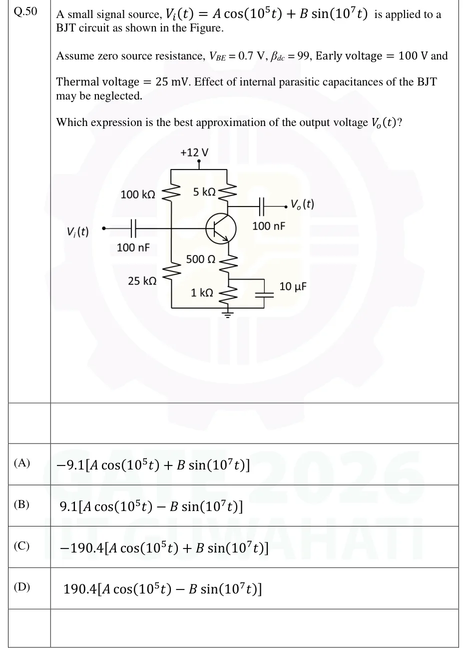
GATE 2026 EC question 50: Single-stage common-emitter amplifier with an NPN BJT.Tap to open full size
Figure from the GATE 2026 EC paper. It is part of the question.
Figure description

Single-stage common-emitter amplifier with an NPN BJT. Supply rail +12 V at the top. Base bias divider: 100 kΩ from +12 V to the base node, 25 kΩ from the base node to ground. The source V_i(t) connects to the base node through a series 100 nF coupling capacitor. Collector: 5 kΩ from +12 V to the collector. The output V_o(t) is taken from the collector through a series 100 nF coupling capacitor, with no load resistor shown (open output terminal). Emitter: 500 Ω from the emitter to an intermediate node, then 1 kΩ from that node to ground. A 10 µF capacitor is connected from the intermediate node (junction of 500 Ω and 1 kΩ) to ground, so it bypasses only the 1 kΩ resistor. The bottom of the 25 kΩ, the 1 kΩ and the 10 µF share the ground.

  1. (A)

  2. (B)

  3. (C)

  4. (D)

Answer and solution
GATE 2026 EC Q.50: answer and solution

GATE 2025 EC Q.21

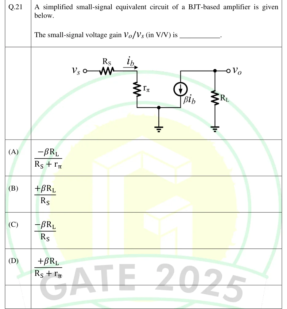
GATE 2025 · ECQ.21 · 1 mark · MCQ

A simplified small-signal equivalent circuit of a BJT-based amplifier is given below.

The small-signal voltage gain (in V/V) is ________.

GATE 2025 EC question 21: Small-signal hybrid-pi circuit.Tap to open full size
Figure from the GATE 2025 EC paper. It is part of the question.
Figure description

Small-signal hybrid-pi circuit. Input side: source terminal v_s (open circle) connects through series resistor R_S to a node; an arrow labelled i_b points rightwards along the wire after R_S, into that node. From that node, resistor r_π goes vertically down to a bottom node that is grounded (ground symbol below a junction dot). Output side: the same grounded bottom node connects to the bottom terminal of a dependent current source labelled β i_b; the arrow inside the source points DOWNWARD (current flows from the top terminal to the bottom/ground terminal). The top terminal of the current source connects to the output node v_o (junction dot, open-circle output terminal labelled v_o). From the output node, load resistor R_L goes down to a separate ground symbol. There is no direct connection between the input node and the output node other than through ground.

  1. (A)

  2. (B)

  3. (C)

  4. (D)

Answer and solution
GATE 2025 EC Q.21: answer and solution

GATE 2025 EC Q.30

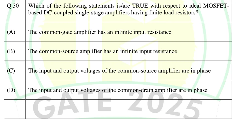
GATE 2025 · ECQ.30 · 1 mark · MSQ

Which of the following statements is/are TRUE with respect to ideal MOSFET-based DC-coupled single-stage amplifiers having finite load resistors?

  1. (A)

    The common-gate amplifier has an infinite input resistance

  2. (B)

    The common-source amplifier has an infinite input resistance

  3. (C)

    The input and output voltages of the common-source amplifier are in phase

  4. (D)

    The input and output voltages of the common-drain amplifier are in phase

Answer and solution
See the question in the paper
GATE 2025 EC Q.30: answer and solution

GATE 2025 EC Q.43

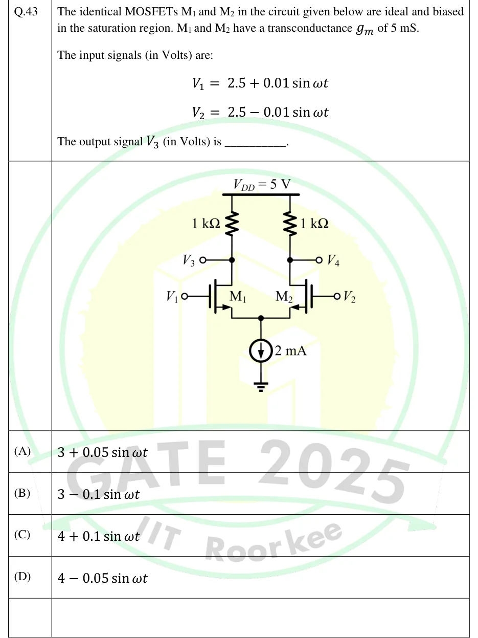
GATE 2025 · ECQ.43 · 2 marks · MCQ

The identical MOSFETs M and M in the circuit given below are ideal and biased in the saturation region. M and M have a transconductance of 5 mS.

The input signals (in Volts) are:


The output signal (in Volts) is ________.

GATE 2025 EC question 43: NMOS differential pair.Tap to open full size
Figure from the GATE 2025 EC paper. It is part of the question.
Figure description

NMOS differential pair. Supply rail V_DD = 5 V at the top. Two 1 kΩ drain resistors hang from V_DD: the left one to the drain of M1, the right one to the drain of M2. The drain node of M1 is brought out as output V3 (terminal on the left); the drain node of M2 is brought out as output V4 (terminal on the right). M1 (n-channel enhancement MOSFET, arrow on the source) has its gate driven by input V1 from the left; M2 (identical n-channel MOSFET) has its gate driven by input V2 from the right. The sources of M1 and M2 are tied together at a common node, which connects to an ideal DC current source of 2 mA pointing downward (current flowing from the common source node to ground), whose lower terminal is grounded.

  1. (A)

  2. (B)

  3. (C)

  4. (D)

Answer and solution
GATE 2025 EC Q.43: answer and solution

GATE 2025 EE Q.16

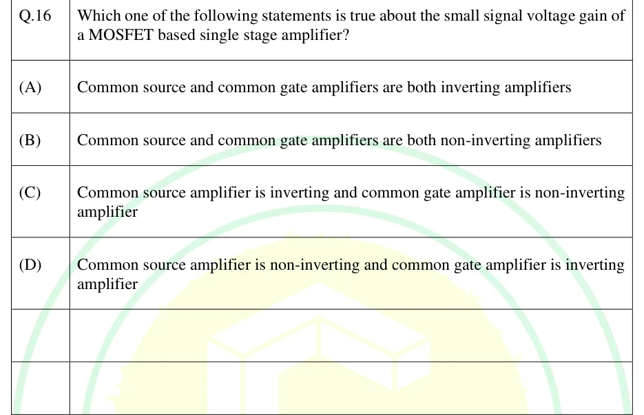
GATE 2025 · EEQ.16 · 1 mark · MCQ

Which one of the following statements is true about the small signal voltage gain of a MOSFET based single stage amplifier?

  1. (A)

    Common source and common gate amplifiers are both inverting amplifiers

  2. (B)

    Common source and common gate amplifiers are both non-inverting amplifiers

  3. (C)

    Common source amplifier is inverting and common gate amplifier is non-inverting amplifier

  4. (D)

    Common source amplifier is non-inverting and common gate amplifier is inverting amplifier

Answer and solution
See the question in the paper
GATE 2025 EE Q.16: answer and solution

GATE 2025 EE Q.38

GATE 2025 · EEQ.38 · 2 marks · MCQ

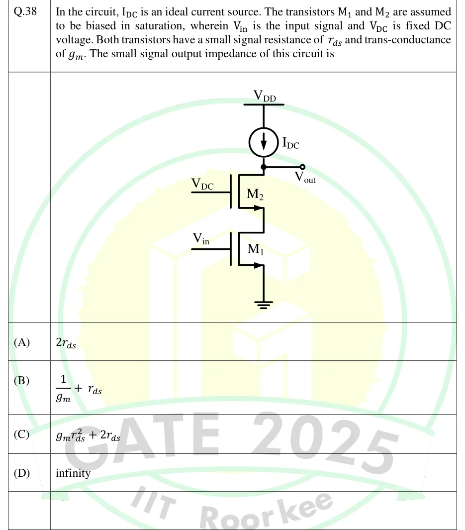
In the circuit, is an ideal current source. The transistors and are assumed to be biased in saturation, wherein is the input signal and is fixed DC voltage. Both transistors have a small signal resistance of and trans-conductance of . The small signal output impedance of this circuit is

GATE 2025 EE question 38: NMOS cascode stage.Tap to open full size
Figure from the GATE 2025 EE paper. It is part of the question.
Figure description

NMOS cascode stage. From the V_DD rail an ideal current source I_DC (arrow pointing down) feeds a node that is brought out as the output terminal V_out. That node is the drain of NMOS M_2 (upper transistor), whose gate is at the fixed DC voltage V_DC. The source of M_2 (arrow on source) goes to the drain of NMOS M_1 (lower transistor), whose gate is driven by the input V_in. The source of M_1 is grounded. No resistors appear anywhere in the circuit.

  1. (A)

  2. (B)

  3. (C)

  4. (D)

    infinity

Answer and solution
GATE 2025 EE Q.38: answer and solution

GATE 2024 EC Q.17

GATE 2024 · ECQ.17 · 1 mark · MCQ

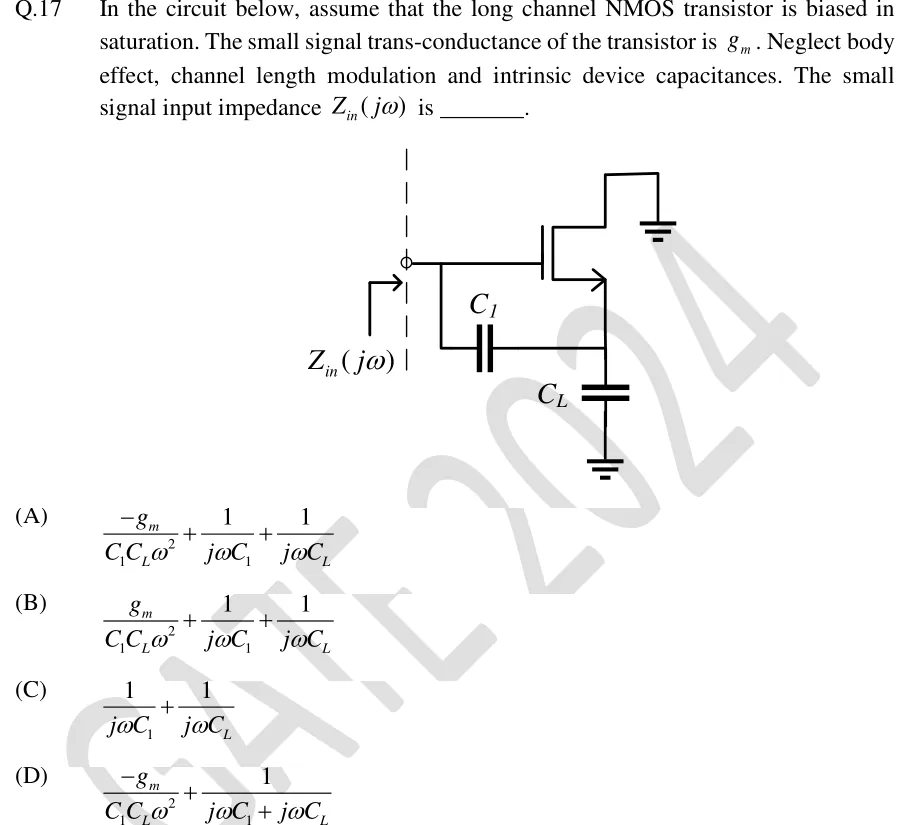
In the circuit below, assume that the long channel NMOS transistor is biased in saturation. The small signal trans-conductance of the transistor is . Neglect body effect, channel length modulation and intrinsic device capacitances. The small signal input impedance is ________.

GATE 2024 EC question 17: An NMOS transistor.Tap to open full size
Figure from the GATE 2024 EC paper. It is part of the question.
Figure description

An NMOS transistor. Its drain goes to ground (drawn at the top right, going to a ground symbol). Its gate connects to the input node, marked with a small open circle on a dashed vertical line. An arrow labelled Z_in(j ω) points into this node. The source (arrow on the source lead, pointing out) connects to a node X. Capacitor C_1 runs from the gate/input node to node X, so it sits between gate and source. Capacitor C_L runs from node X to ground. No resistors or other components; bias is not shown (the device is assumed to be in saturation).

  1. (A)

  2. (B)

  3. (C)

  4. (D)

Answer and solution
GATE 2024 EC Q.17: answer and solution

GATE 2024 EC Q.51

GATE 2024 · ECQ.51 · 2 marks · MCQ

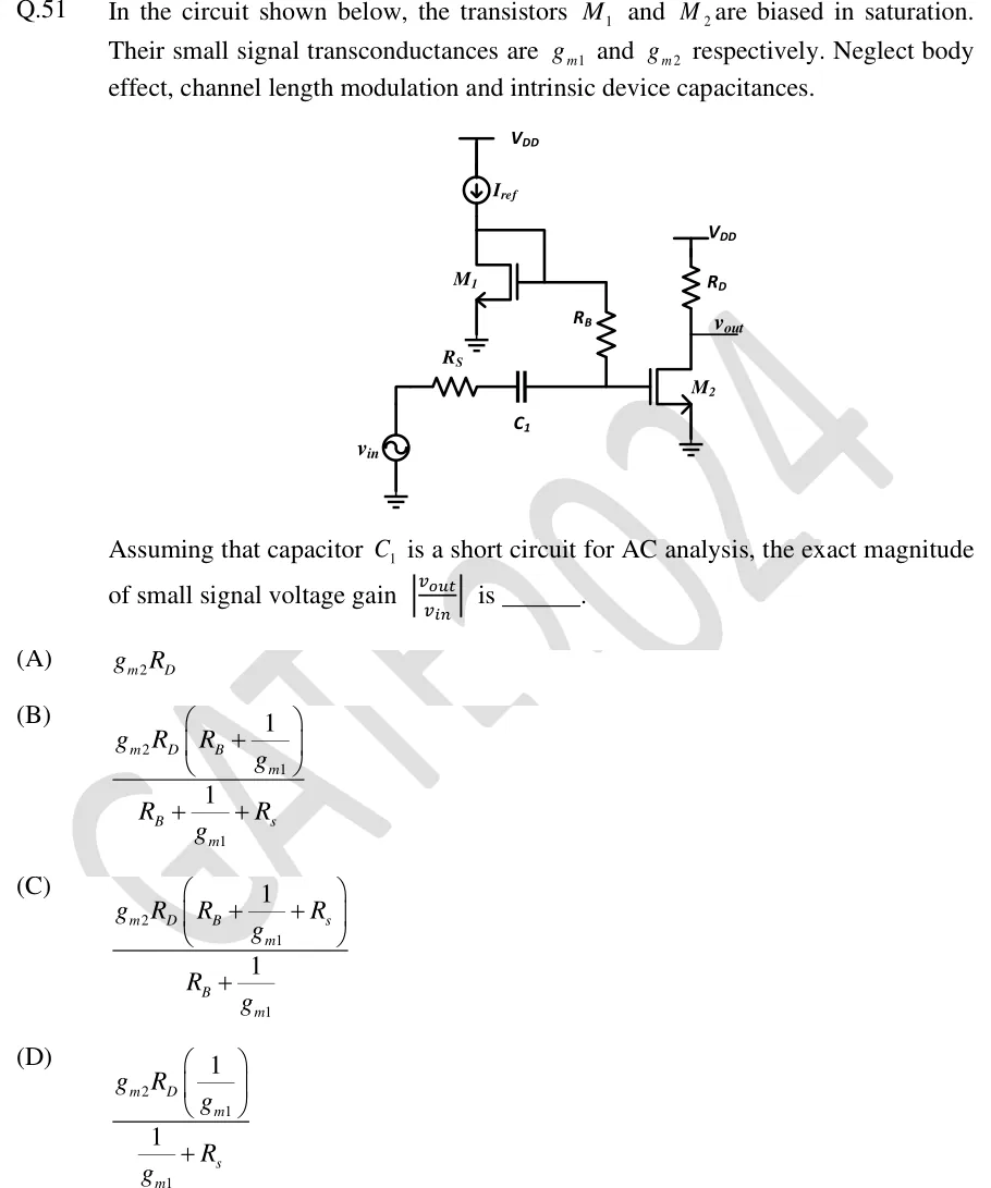
In the circuit shown below, the transistors and are biased in saturation. Their small signal transconductances are and respectively. Neglect body effect, channel length modulation and intrinsic device capacitances.

[Figure]

Assuming that capacitor is a short circuit for AC analysis, the exact magnitude of small signal voltage gain is ______.

GATE 2024 EC question 51: Two NMOS transistors.Tap to open full size
Figure from the GATE 2024 EC paper. It is part of the question.
Figure description

Two NMOS transistors. Left branch: a current source I_ref (arrow pointing down) from V_DD feeds the drain of NMOS M_1; the source of M_1 is grounded. The drain of M_1 is tied by a wire to the gate of M_1 (diode-connected), and this same drain/gate node connects to the top of resistor R_B. The bottom of R_B goes to the gate of NMOS M_2. Input: an AC source v_in (bottom terminal grounded) in series with resistor R_S and capacitor C_1, the far side of C_1 connected to the gate of M_2 (same node as the bottom of R_B). Right branch: M_2 source grounded, drain connected through R_D to V_DD; the output v_out is taken at the drain of M_2.

  1. (A)

  2. (B)

  3. (C)

  4. (D)

Answer and solution
GATE 2024 EC Q.51: answer and solution

GATE 2023 EC Q.21

GATE 2023 · ECQ.21 · 1 mark · MCQ

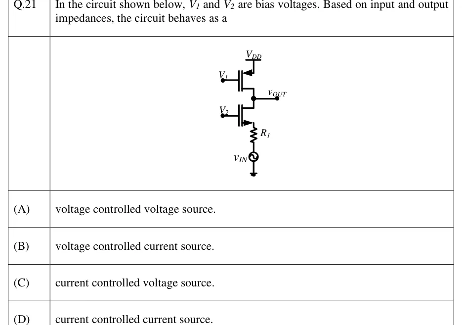
In the circuit shown below, and are bias voltages. Based on input and output impedances, the circuit behaves as a

GATE 2023 EC question 21: Two MOSFETs are stacked in series between V_DD and the input source.Tap to open full size
Figure from the GATE 2023 EC paper. It is part of the question.
Figure description

Two MOSFETs are stacked in series between V_DD and the input source. Top device: a PMOS whose source is connected to V_DD (the source arrow points into the device) and whose gate is driven by the DC bias V_1. Its drain goes to the output node, marked v_OUT. Bottom device: an NMOS whose gate is driven by the DC bias V_2 and whose drain is connected to the same output node v_OUT. Its source (the arrow points out) connects to one end of a resistor R_1. The other end of R_1 goes to the top terminal of an AC voltage source v_IN (a circle with a tilde, no polarity marks), whose bottom terminal is grounded. So v_IN, through the series resistor R_1, drives the NMOS source, and the output is taken at the common drain node of the NMOS and the PMOS.

  1. (A)

    voltage controlled voltage source.

  2. (B)

    voltage controlled current source.

  3. (C)

    current controlled voltage source.

  4. (D)

    current controlled current source.

Answer and solution
GATE 2023 EC Q.21: answer and solution

GATE 2023 EC Q.64

GATE 2023 · ECQ.64 · 2 marks · NAT

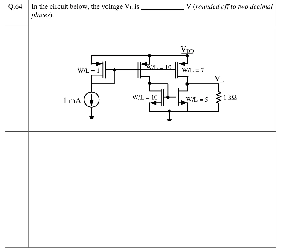
In the circuit below, the voltage is ________ V (rounded off to two decimal places).

GATE 2023 EC question 64: A CMOS current-mirror circuit, supply V_DD on a top rail and ground at the bottom.Tap to open full size
Figure from the GATE 2023 EC paper. It is part of the question.
Figure description

A CMOS current-mirror circuit, supply V_DD on a top rail and ground at the bottom. Three PMOS transistors have their sources on the V_DD rail and share one gate line. (1) Left PMOS M_1, W/L = 1: diode-connected (gate tied to drain). Its drain goes to a 1 mA current source that pulls current down to ground. (2) Middle PMOS M_2, W/L = 10: gate on the shared gate line, drain at node X. (3) Right PMOS M_3, W/L = 7: gate on the shared gate line, drain at the output node V_L. Two NMOS transistors below have their sources grounded. (4) Left NMOS M_4, W/L = 10: drain at node X. Node X is also wired to the common gate of M_4 and M_5, so M_4 is diode-connected. (5) Right NMOS M_5, W/L = 5: gate on that common gate node, drain at the output node V_L. A 1 kΩ load resistor runs from V_L to ground.

Answer and solution
GATE 2023 EC Q.64: answer and solution

GATE 2023 IN Q.56

GATE 2023 · INQ.56 · 2 marks · NAT

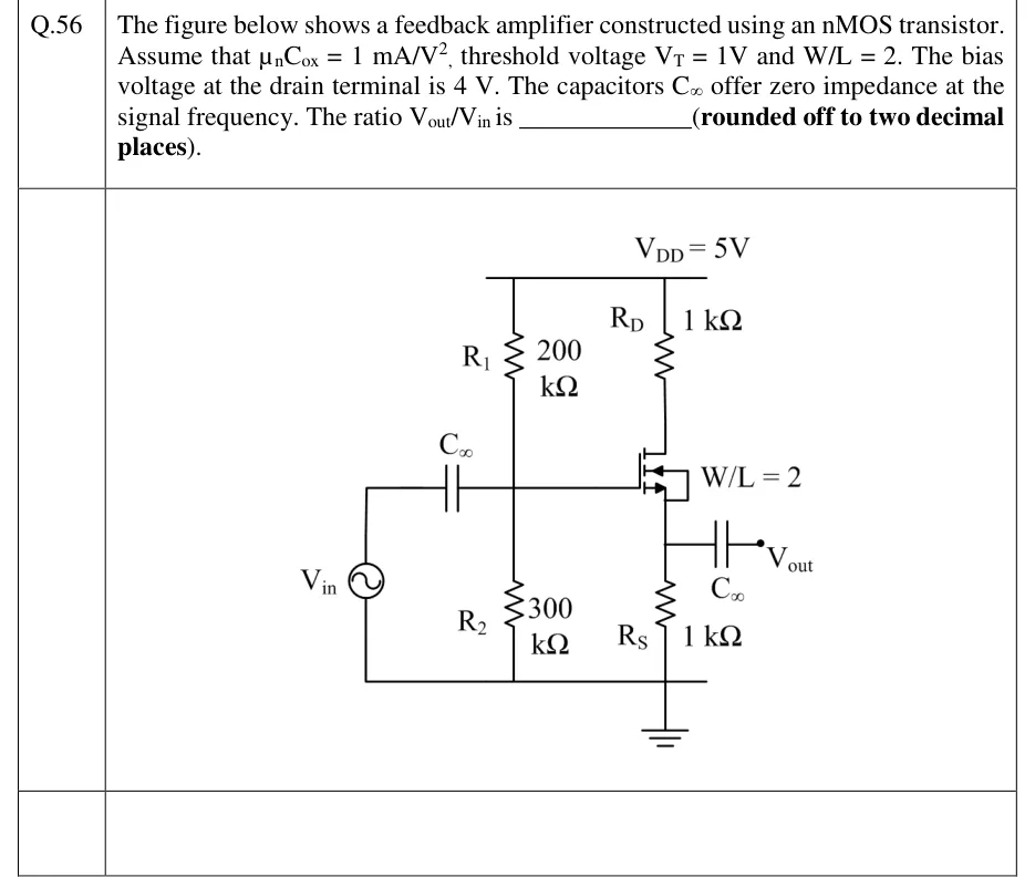
The figure below shows a feedback amplifier constructed using an nMOS transistor. Assume that , threshold voltage and . The bias voltage at the drain terminal is 4 V. The capacitors offer zero impedance at the signal frequency. The ratio is ________ (rounded off to two decimal places).

GATE 2023 IN question 56: A single enhancement nMOS stage with supply V_DD = 5 V at the top rail.Tap to open full size
Figure from the GATE 2023 IN paper. It is part of the question.
Figure description

A single enhancement nMOS stage with supply V_DD = 5 V at the top rail. R_D = 1 kΩ connects V_DD to the drain. The gate is biased by a divider: R_1 = 200 kΩ from V_DD to the gate node and R_2 = 300 kΩ from the gate node to ground. A source V_in (sinusoidal symbol, lower terminal grounded) drives the gate node through a coupling capacitor C∞. The body (substrate) is tied to the source, shown by the arrow connected to the source terminal; the device is labelled W/L = 2. R_S = 1 kΩ connects the source to ground. The output V_out is taken from the source node through a second coupling capacitor C∞, with no load drawn. All grounds (V_in return, R_2, R_S) are common.

Answer and solution
GATE 2023 IN Q.56: answer and solution

GATE 2022 EC Q.59

GATE 2022 · ECQ.59 · 2 marks · NAT

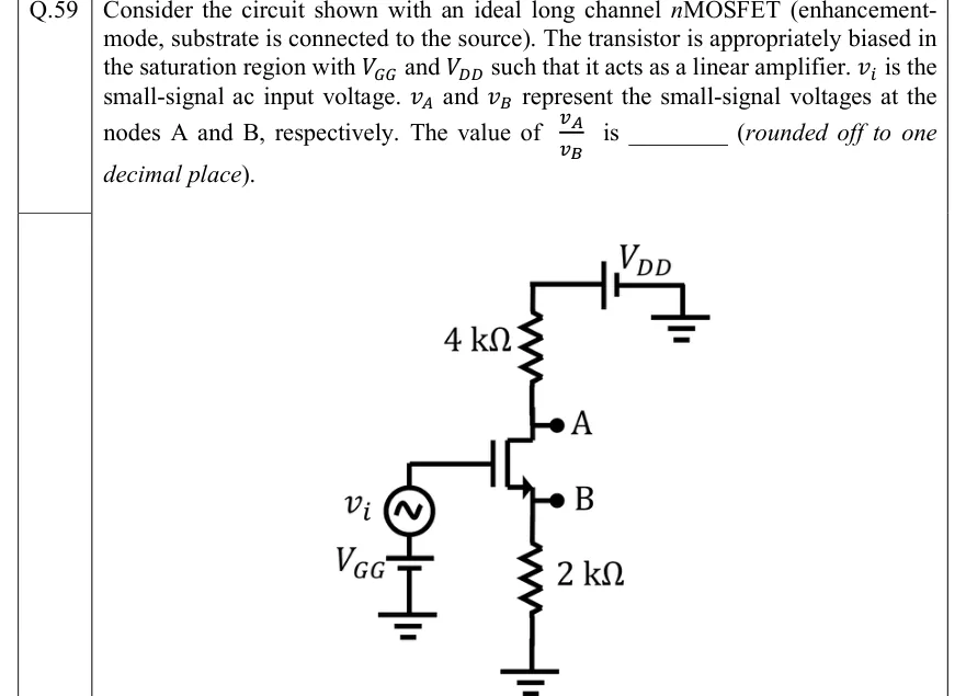
Consider the circuit shown with an ideal long channel MOSFET (enhancement-mode, substrate is connected to the source). The transistor is appropriately biased in the saturation region with and such that it acts as a linear amplifier. is the small-signal ac input voltage. and represent the small-signal voltages at the nodes A and B, respectively. The value of is ________ (rounded off to one decimal place).

GATE 2022 EC question 59: Enhancement-mode n-channel MOSFET, body tied to source.Tap to open full size
Figure from the GATE 2022 EC paper. It is part of the question.
Figure description

Enhancement-mode n-channel MOSFET, body tied to source. Gate is driven by an ac source v_i in series with a dc battery V_GG whose negative terminal is grounded (v_i on top, connected to the gate; V_GG below, to ground). Drain connects through a 4 kΩ resistor up to the positive terminal of a dc supply V_DD whose other terminal is grounded. The drain node is labelled A. The source node is labelled B and connects through a 2 kΩ resistor to ground. Nodes: A = drain, B = source.

Answer and solution
GATE 2022 EC Q.59: answer and solution

GATE 2022 IN Q.44

GATE 2022 · INQ.44 · 2 marks · MCQ

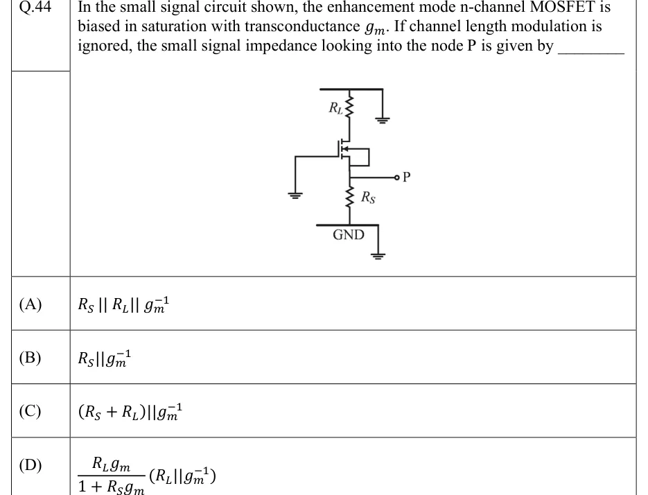
In the small signal circuit shown, the enhancement mode n-channel MOSFET is biased in saturation with transconductance . If channel length modulation is ignored, the small signal impedance looking into the node P is given by ________

GATE 2022 IN question 44: An enhancement-mode n-channel MOSFET (broken channel line, arrow on the body terminal pointing inward).Tap to open full size
Figure from the GATE 2022 IN paper. It is part of the question.
Figure description

An enhancement-mode n-channel MOSFET (broken channel line, arrow on the body terminal pointing inward). The drain connects upward through resistor R_L to a top horizontal rail; that rail extends to the right and ends in a ground symbol (so it is small-signal ground). The gate connects by a wire going left and then down to a ground symbol. The body terminal is tied directly to the source by a short bracket wire on the right side of the transistor. The source node is brought out to the right as the terminal marked P. From the source node, resistor R_S goes down to a bottom horizontal rail labelled GND, which ends on the right in a ground symbol.

  1. (A)

  2. (B)

  3. (C)

  4. (D)

Answer and solution
GATE 2022 IN Q.44: answer and solution

GATE 2022 IN Q.47

GATE 2022 · INQ.47 · 2 marks · MCQ

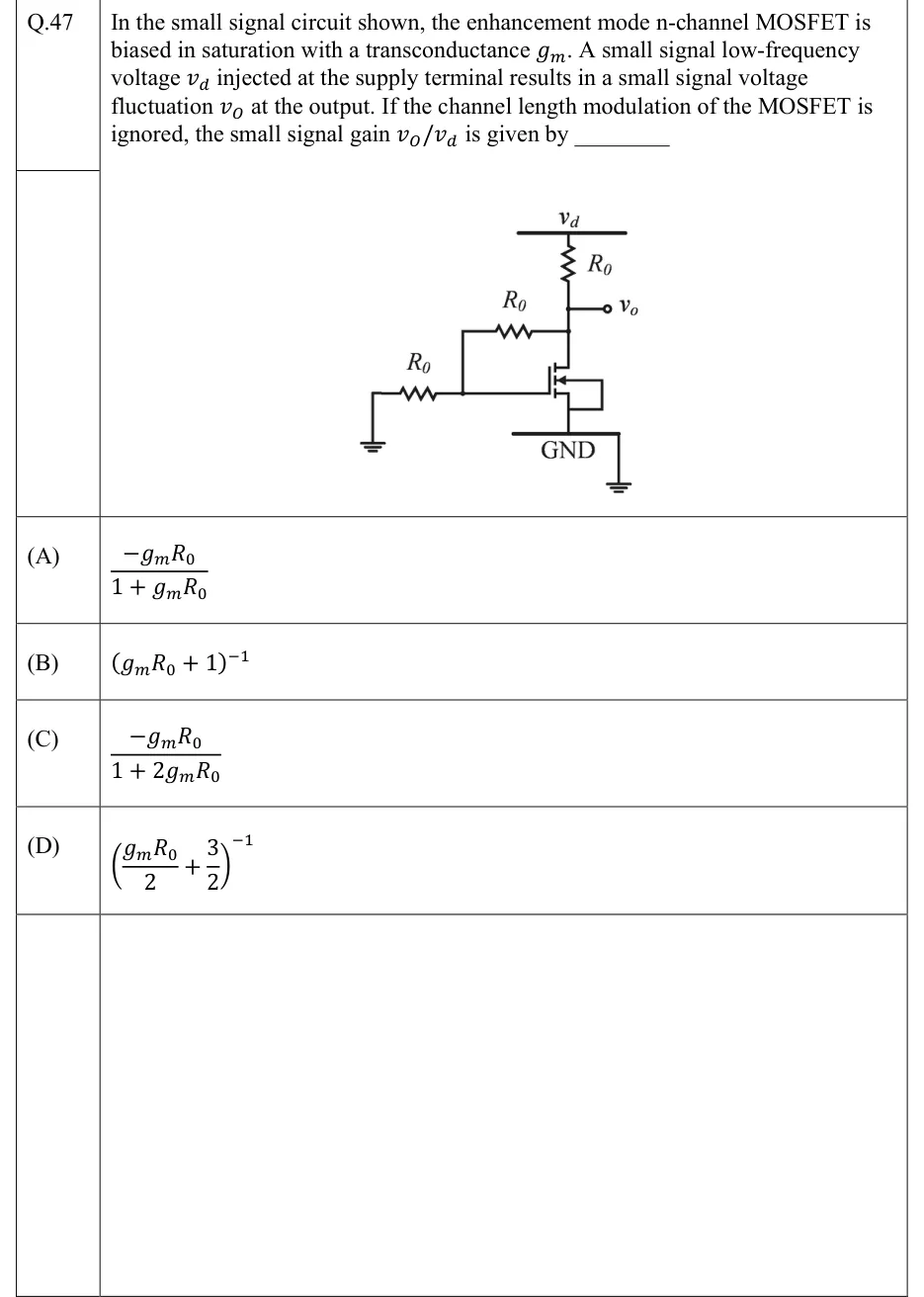
In the small signal circuit shown, the enhancement mode n-channel MOSFET is biased in saturation with a transconductance . A small signal low-frequency voltage injected at the supply terminal results in a small signal voltage fluctuation at the output. If the channel length modulation of the MOSFET is ignored, the small signal gain is given by ________

GATE 2022 IN question 47: Small-signal circuit with one enhancement-mode n-channel MOSFET (body arrow pointing into the channel;Tap to open full size
Figure from the GATE 2022 IN paper. It is part of the question.
Figure description

Small-signal circuit with one enhancement-mode n-channel MOSFET (body arrow pointing into the channel; body tied to the source). A horizontal supply rail at the top is labelled v_d. A resistor R_0 runs from the v_d rail down to the drain node. The drain node is also the output terminal v_o (open circle to the right). A second resistor R_0 runs from the drain node across to the gate node (drain-to-gate feedback resistor). A third resistor R_0 runs from the gate node to ground (ground symbol at the left). The source, together with the body, connects to the bottom rail labelled GND, which is grounded. All three resistors are equal, R_0.

  1. (A)

  2. (B)

  3. (C)

  4. (D)

Answer and solution
GATE 2022 IN Q.47: answer and solution

GATE 2020 EC Q.35

GATE 2020 · ECQ.35 · 2 marks · MCQ

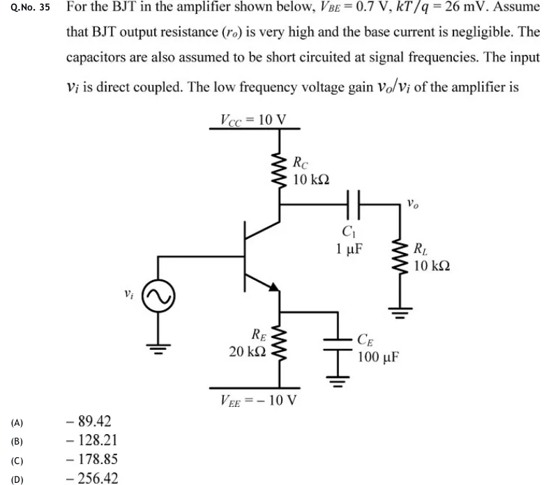
For the BJT in the amplifier shown below, , . Assume that BJT output resistance () is very high and the base current is negligible. The capacitors are also assumed to be short circuited at signal frequencies. The input is direct coupled. The low frequency voltage gain of the amplifier is

GATE 2020 EC question 35: Common-emitter amplifier with an NPN BJT and split supplies.Tap to open full size
Figure from the GATE 2020 EC paper. It is part of the question.
Figure description

Common-emitter amplifier with an NPN BJT and split supplies. The collector connects through R_C = 10 k Ω to V_CC = 10 V. The emitter (arrow pointing out, NPN) connects through R_E = 20 k Ω to V_EE = -10 V; a bypass capacitor C_E = 100 connects from the emitter to ground. The base is driven directly (no coupling capacitor, no bias resistors) by an AC source v_i whose other terminal is grounded. The collector is coupled through C_1 = 1 to the output node v_o, which is loaded by R_L = 10 k Ω to ground.

  1. (A)

  2. (B)

  3. (C)

  4. (D)

Answer and solution
GATE 2020 EC Q.35: answer and solution

GATE 2020 EC Q.37

GATE 2020 · ECQ.37 · 2 marks · MCQ

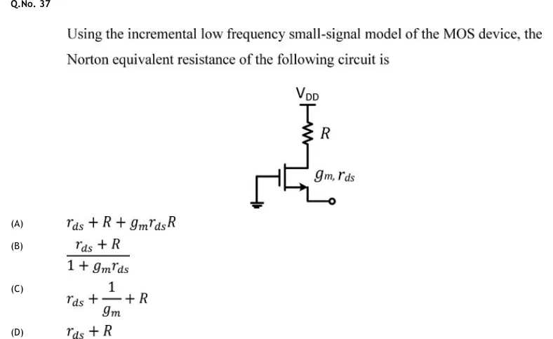
Using the incremental low frequency small-signal model of the MOS device, the Norton equivalent resistance of the following circuit is

GATE 2020 EC question 37: One n-channel MOSFET, drawn as a three-terminal symbol with the arrow on the source pointing outward and labelled with its…Tap to open full size
Figure from the GATE 2020 EC paper. It is part of the question.
Figure description

One n-channel MOSFET, drawn as a three-terminal symbol with the arrow on the source pointing outward and labelled with its small-signal parameters g_m, r_ds. The gate lead runs left and is wired directly to ground. The drain (top) goes through a resistor R up to the supply V_DD. The source (bottom) is brought out to the right to an open terminal (small circle). The Norton equivalent is taken at this source terminal. There are no other components.

  1. (A)

  2. (B)

  3. (C)

  4. (D)

Answer and solution
GATE 2020 EC Q.37: answer and solution

GATE 2018 EC Q.1

GATE 2018 · ECQ.1 · 1 mark · MCQ

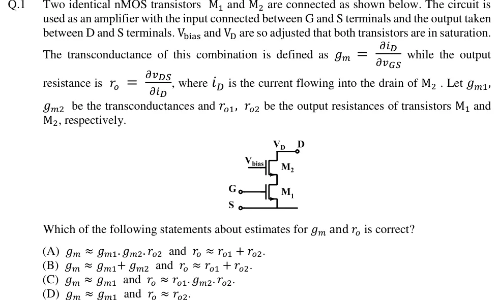
Two identical nMOS transistors and are connected as shown below. The circuit is used as an amplifier with the input connected between G and S terminals and the output taken between D and S terminals. and are so adjusted that both transistors are in saturation. The transconductance of this combination is defined as while the output resistance is , where is the current flowing into the drain of . Let , be the transconductances and , be the output resistances of transistors and , respectively.

Which of the following statements about estimates for and is correct?

GATE 2018 EC question 1: Two nMOS transistors stacked in series (cascode).Tap to open full size
Figure from the GATE 2018 EC paper. It is part of the question.
Figure description

Two nMOS transistors stacked in series (cascode). Upper transistor M2: its gate is driven by a DC voltage labelled V_bias; its drain goes up to the output terminal labelled D, at voltage V_D. The source of M2 connects directly to the drain of lower transistor M1. Lower transistor M1: its gate connects to the input terminal G; its source connects to terminal S, which is the common (ground) rail running along the bottom. Input is applied between G and S; output is taken between D and S. Both transistors are drawn as enhancement nMOS with arrows on the source leads; the body connections are not drawn separately.

  1. (A)

    and .

  2. (B)

    and .

  3. (C)

    and .

  4. (D)

    and .

Answer and solution
GATE 2018 EC Q.1: answer and solution

PRACTICE

5 questions to test yourself

PRACTICE 12 marks · NAT

A Widlar current source uses two matched NPN transistors. The diode-connected transistor Q1 carries mA, and a resistor is placed in the emitter of the output transistor Q2 only. Take mV, neglect base currents and the Early effect, and assume Q2 stays in the active region. For an output current μA, the required value of in kΩ is ______ (round off to two decimal places).

Answer and solution

Answer: (accepted range )

  1. KVL around the two base-emitter junctions gives , taking Q2's emitter current as since base currents are neglected.

  2. For matched transistors, .

  3. Ω ≈ 11 513 Ω = 11.51 kΩ.

PRACTICE 22 marks · NAT

A BJT differential pair uses identical transistors with and collector resistors kΩ. It is biased by a tail current source of mA whose output resistance is kΩ. Take mV, neglect of the pair's transistors, and assume small-signal operation. With the output taken single-ended from one collector, the CMRR in dB is ______ (round off to two decimal places).

Answer and solution

Answer: (accepted range )

  1. Each transistor carries mA, so mA/V and Ω.

  2. Single-ended differential gain: .

  3. The common-mode half-circuit has kΩ in the emitter: .

  4. , which is dB. The shortcut gives the same value to two decimals.

PRACTICE 31 mark · NAT

An NMOS common-source amplifier has its source at AC ground (fully bypassed) and is biased in saturation at mA with overdrive voltage V. The drain resistor is kΩ, the transistor's output resistance is kΩ, and there is no external load. Using the square-law model, the magnitude of the midband small-signal voltage gain from gate to drain is ______ (round off to two decimal places).

Answer and solution

Answer: (accepted range )

  1. mA/V.

  2. Total drain load: kΩ.

  3. .

PRACTICE 41 mark · MCQ

A BJT common-emitter stage, with its emitter at AC ground, has pF and pF. Its midband small-signal voltage gain from base to collector, including the load, is . Using Miller's theorem, the total capacitance from the base to ground is

  1. (A)

    22 pF

  2. (B)

    100 pF

  3. (C)

    118 pF

  4. (D)

    120 pF

Answer and solution

Answer: (D)

  1. Miller's theorem: , connected between base and collector with , appears at the base as pF.

  2. already runs from the base to the AC-grounded emitter, so the two add: pF.

  3. 118 pF comes from using instead of ; 100 pF leaves out ; 22 pF ignores the Miller effect.

PRACTICE 52 marks · MSQ

Which of the following statements are correct? Assume matched transistors, small-signal operation where relevant, and neglected unless a statement mentions it.

  1. (A)

    In a basic two-transistor BJT current mirror with identical transistors of current gain , the output current is when the Early effect is neglected.

  2. (B)

    In a BJT cascode amplifier (a CE stage driving a CB stage, both at the same collector current), the base-collector capacitance of the CE transistor is Miller-multiplied by only about 2. This is why the cascode has a higher upper cut-off frequency than a single CE stage with the same source and load resistances.

  3. (C)

    In an NMOS differential pair biased by a tail current (square-law devices, overdrive at ), all of flows in one transistor only once , and not at any smaller differential input.

  4. (D)

    For a BJT differential pair with resistive collector loads, doubling the tail current halves the differential voltage gain, provided all transistors stay active and the load resistors are unchanged.

Answer and solution

Answer: (A), (B)

  1. A: KCL at the reference node gives (Q1's collector current plus two base currents), and . So . Correct.

  2. B: Q1's collector sees Q2's emitter, about . Q1's gain is therefore about , and appears at the input as instead of . Correct.

  3. C: At balance . Full switching needs one device at (to carry ) and the other at threshold, so is already enough. Incorrect.

  4. D: with . Doubling doubles and therefore doubles . Incorrect.

OFFICIAL GATE 2027 SYLLABUS WORDING

Copied from the GATE 2027 syllabus; see all 2027 syllabi.

GATE EC

AC coupling, small signal analysis, frequency response. Current mirrors and differential amplifiers

GATE EE

equivalent circuit and frequency response

GATE IN

small signal analysis, frequency response of transistor circuits … amplifier design

Preparing in Kolkata? IAE Academy's course for GATE ECE, GATE EE or GATE IN.