Feedback amplifiers and oscillators are one loop read two ways. With negative feedback (Aβ>0 in the mid-band) the closed-loop gain A/(1+Aβ) gives up raw gain in exchange for a stable gain, wider bandwidth, lower distortion, and input and output resistances set by the topology. With positive feedback, a loop gain of exactly 1 at zero phase sustains a sinusoidal oscillation; a relaxation oscillator instead switches between two states at a rate set by an RC time constant. These notes show how to identify a topology from a circuit, work out closed-loop gain, resistances, bandwidth and sensitivity, and find an oscillator's frequency and the minimum gain it needs.
4 previous-year questions · 4 solved · 6 practice questions
Negative feedback: the basic loop
A feedback amplifier samples its output xo and passes it through a feedback network with transfer ratio β, so xf=βxo. The result is subtracted from the source: the basic amplifier sees xi=xs−xf and delivers xo=Axi. Here x is a voltage or a current, depending on the topology, and A and β carry whatever units make the product Aβ dimensionless.
The loop gainT=Aβ is the gain once round the loop. To find it, set xs=0, break the loop at the amplifier input and inject a test signal xt: the signal that comes back is −Aβxt. Feedback is negative when Aβ>0 in the mid-band, so that ∣1+Aβ∣>1 and the gain falls. If ∣1+Aβ∣<1 at some frequency, the feedback is positive there. If 1+Aβ=0, the circuit oscillates.
The price is the gain itself. Every improvement described below comes by the factor 1+Aβ, and the gain drops by that same factor.
CLOSED-LOOP GAIN (NEGATIVE FEEDBACK)
Af=xsxo=1+AβA
Convention: xi=xs−xf,xf=βxo. The feedback is negative when Aβ>0 in the mid-band (in general, when ∣1+Aβ∣>1).
LOOP GAIN AND AMOUNT OF FEEDBACK
T=Aβ,D=1+Aβ,gain reduction=20log10∣1+Aβ∣dB
T is the gain once round the loop. Every benefit of negative feedback, and the loss of gain, is by the factor D.
LARGE LOOP GAIN
Af≈β1(Aβ≫1)
Exact form: Af=β1⋅1+AβAβ. So 1/β overstates the true gain by the fraction 1/(Aβ); equivalently, the true gain lies below 1/β by the fraction 1/(1+Aβ).
DESENSITIVITY TO THE AMPLIFIER GAIN
AfdAf=1+Aβ1⋅AdA
A differential result, valid for small changes in A with β fixed; 1+Aβ is also called the desensitivity factor. For a large change, work out Af exactly before and after.
SENSITIVITY TO THE FEEDBACK NETWORK
AfdAf=−1+AβAβ⋅βdβ≈−βdβ
Small changes in β with A fixed; the approximation needs Aβ≫1. The closed-loop gain is only as stable as β. That is why β is built from resistors or capacitors, not from active devices.
EXAM TIP
Books use different sign conventions. With xi=xs−xf the gain is A/(1+Aβ) and the circuit oscillates at Aβ=−1. With xi=xs+xf the gain is A/(1−Aβ) and it oscillates at Aβ=+1. The physics is the same in both, so check which convention a question uses before you substitute.
EXAM TIP
Using 1/β when Aβ is not large costs accuracy. With Aβ=20 the true gain is 20/21 of 1/β, which is 4.8% lower.
What negative feedback buys: bandwidth, distortion and noise
Take an amplifier with a single high-frequency pole, A(s)=AM/(1+s/ωH), and a frequency-independent β. Substituting into A/(1+Aβ) gives Af(s)=1+s/[ωH(1+AMβ)]AM/(1+AMβ). The result still has a single pole: the mid-band gain falls by 1+AMβ and the pole moves up by the same factor. A single low-frequency pole moves down by that factor, so the bandwidth widens at both ends.
UPPER CUTOFF WITH FEEDBACK
AMf=1+AMβAM,ωHf=ωH(1+AMβ)
Amplifier with a single high-frequency pole ωH and mid-band gain AM;β independent of frequency.
LOWER CUTOFF WITH FEEDBACK
ωLf=1+AMβωL
Single low-frequency pole, A(s)=AM/(1+ωL/s);β independent of frequency.
GAIN-BANDWIDTH PRODUCT
AMfωHf=AMωH
Constant for a single-pole amplifier: gain is traded one-for-one for bandwidth. It is not exact when the amplifier has more than one significant pole.
Negative feedback also reduces nonlinear distortion, and noise or hum, that arise inside the loop after the input, typically in the output stage. Measured at the output, such a disturbance is divided by 1+Aβ. The comparison is fair only at the same output signal amplitude: the input must be raised by the factor 1+Aβ to bring the output back up, and the extra gain ahead of the loop that does this is assumed to add no distortion or noise of its own. Noise that enters with the signal at the input is amplified exactly like the signal, so feedback cannot improve the signal-to-noise ratio of the input itself.
DISTORTION AND NOISE GENERATED INSIDE THE LOOP
Vd,f=1+AβVd,Vn,f=1+AβVn
Vd and Vn are the distortion and noise components at the output without feedback, generated inside the loop after the input (for example in the output stage). Vd,f and Vn,f are the same components with feedback, compared at the same output signal amplitude.
EXAM TIP
Feedback does not clean up noise that arrives with the signal. That noise and the signal are scaled by the same Af, so the input signal-to-noise ratio stays the same. Only disturbances injected after the input stage are reduced.
EXAM TIP
With a frequency-independent β, an amplifier with one or two poles (all in the left half-plane) and no zeros stays stable, because the phase of Aβ reaches −180∘ only as ω→∞, where ∣Aβ∣→0. Two poles can still cause gain peaking in the closed-loop response. With three or more poles the phase passes −180∘ at a finite frequency. If ∣Aβ∣≥1 there, the negative-feedback amplifier oscillates.
GAIN MARGIN AND PHASE MARGIN
GM=−20log10∣Aβ(jω180)∣dB,PM=180∘+∠Aβ(jω1)
Negative-feedback convention, with ∠Aβ=0∘ in the mid-band. ω180 is the frequency at which ∠Aβ=−180∘, and ω1 the frequency at which ∣Aβ∣=1. For an amplifier whose open-loop poles all lie in the left half-plane and whose ∣Aβ∣ falls through 1 only once, the feedback amplifier is stable when both margins are positive.
The four feedback topologies
At the output, the feedback network either samples the output voltage (it is connected in shunt across the load) or the output current (it is connected in series with the load). At the input, it either subtracts a voltage (in series with the source) or a current (in shunt at the input node). The name gives the input mixing first and the output sampling second.
Series connections add impedances, so series mixing raises the input resistance and series (current) sampling raises the output resistance. Shunt connections lower them. The factor is always 1+Aβ, with A and β of the type that matches the topology. Each topology pushes the amplifier towards its own ideal: a voltage amplifier wants high Rin and low Rout, a transconductance amplifier wants both high, a transresistance amplifier wants both low, and a current amplifier wants low Rin and high Rout. In a real circuit the β network also loads the basic amplifier. The standard method folds that loading into A (the A circuit) and then applies the ideal formulas.
Topology (mixing–sampling)
Older name
Samples
Mixes
Gain type of A and Af
Units of β
Rin
Rout
Series-shunt
Voltage-series
Output voltage
Voltage, in series
Voltage gain (V/V)
V/V
× (1+Aβ)
÷ (1+Aβ)
Series-series
Current-series
Output current
Voltage, in series
Transconductance (A/V)
V/A = Ω
× (1+Aβ)
× (1+Aβ)
Shunt-shunt
Voltage-shunt
Output voltage
Current, at a node
Transresistance (V/A)
A/V = S
÷ (1+Aβ)
÷ (1+Aβ)
Shunt-series
Current-shunt
Output current
Current, at a node
Current gain (A/A)
A/A
÷ (1+Aβ)
× (1+Aβ)
INPUT RESISTANCE, SERIES MIXING
Rif=Ri(1+Aβ)
The feedback voltage is in series with the source. Ri is the input resistance of the basic amplifier.
INPUT RESISTANCE, SHUNT MIXING
Rif=1+AβRi
The feedback current is added at the input node.
OUTPUT RESISTANCE, VOLTAGE (SHUNT) SAMPLING
Rof=1+AβRo
Here A is the open-circuit (load removed) gain of the basic amplifier, because its output is modelled as a Thevenin source.
OUTPUT RESISTANCE, CURRENT (SERIES) SAMPLING
Rof=Ro(1+Aβ)
Here A is the short-circuit (load shorted) gain of the basic amplifier, because its output is modelled as a Norton source.
EXAM TIP
The factor 1+Aβ applies only to a resistance measured at a point inside the loop. A bias resistor that shunts the input of a series-mixed stage, or the collector resistor RC in parallel with the output of a current-sampled stage, is outside the loop and is combined in parallel afterwards. For example, in a CE stage with unbypassed RE the resistance looking into the collector rises, but the output resistance of the stage is still about RC.
WORKED EXAMPLE · WORKED EXAMPLE 1: SERIES-SHUNT AMPLIFIER
A voltage amplifier has open-circuit voltage gain A=2000, input resistance Ri=4kΩ, output resistance Ro=1kΩ and a single high-frequency pole at 25 kHz. It is placed in a series-shunt negative-feedback loop with an ideal, non-loading β network, no load is connected, and the closed-loop gain is 40. Find (a) β, (b) Rif and Rof, (c) the closed-loop upper 3-dB frequency, and (d) the change in closed-loop gain if A falls by 10%.
▸ Solution
(a) Af=A/(1+Aβ)=40, so 1+Aβ=2000/40=50,Aβ=49 and β=49/2000=0.0245.
(b) Series mixing: Rif=Ri(1+Aβ)=4kΩ×50=200kΩ. Voltage sampling (A is the open-circuit gain, as given): Rof=Ro/(1+Aβ)=1000/50=20Ω.
(c) Single pole: fHf=fH(1+Aβ)=25kHz×50=1.25MHz. Check: 2000×25kHz=40×1.25MHz=50MHz.
Exact: with A=1800,1+Aβ=1+1800×0.0245=45.1 and Af=1800/45.1=39.911, a change of −0.222%.
Answer:β=0.0245;Rif=200kΩ,Rof=20Ω;fHf=1.25MHz. A 10% drop in A moves Af from 40 to 39.91, about −0.22% (the differential estimate gives −0.2%).
Identifying the topology from a circuit
Find the feedback network: the element or elements that carry a signal from the output side back to the input side. This may be a resistor RF, an unbypassed emitter or source resistor shared by the input and output loops, or a divider feeding an op-amp input.
Sampling: short the output (vo=0). If the feedback signal disappears, the output voltage is sampled (shunt, or voltage, sampling). Open the output loop (io=0). If the feedback signal disappears, the output current is sampled (series, or current, sampling). In practice, feedback taken from the output node itself is voltage sampling, and feedback taken from a resistor that carries the output current is current sampling.
Mixing: if the feedback returns to the same node that receives the input signal, currents add at that node and the mixing is shunt. Examples: the base, when the signal drives the base; the inverting input, when the signal enters through R1 at the inverting input. If it returns to the other terminal of the input port, the feedback voltage subtracts around the input loop and the mixing is series. Examples: the emitter or source, when the signal drives the base or gate; the inverting input, when the signal drives the non-inverting input.
Check the sign by tracing a small increase at the input around the loop: the feedback must oppose it. For a BJT, feedback to the base must come from a point in antiphase with the base, and feedback to the emitter must come from a point in phase with the base.
Name the topology mixing first and sampling second, then apply the matching A,β and resistance rules.
Circuit
Topology
Feedback factor β
Closed-loop result (large loop gain)
Non-inverting op-amp amplifier (R1 to ground, R2 feedback)
Series-shunt
R1/(R1+R2)
vo/vs=1+R2/R1
Voltage follower, emitter follower, source follower
Series-shunt
1
vo/vs≈1
Two CE stages, RF from Q2 collector to Q1 emitter (RE1 to ground)
Series-series feedback. Hybrid-π model with gm=IC/VT (VT=25mV at room temperature if a number is needed) and rπ=hfe/gm; the current gain is written hfe to keep β for the feedback factor; ro neglected; no source resistance; output at the collector, with RC the total collector load. The approximation holds when (1+hfe)RE≫rπ and hfe≫1. Input resistance looking into the base: rπ+(1+hfe)RE.
EXAM TIP
Two naming systems are in use. Series-shunt (mixing, then sampling) is the same topology as voltage-series (sampled quantity, then mixing). Likewise series-series = current-series, shunt-shunt = voltage-shunt, and shunt-series = current-shunt. If a question uses the words voltage or current, it is using the older system, and the first word is the output sampling.
Oscillators: the Barkhausen criterion and amplitude control
An oscillator is a feedback loop that supplies its own input. In the positive-feedback convention xi=xs+xf, the closed-loop gain is A/(1−Aβ). At a frequency where Aβ=1 this gain is infinite, which means an output can exist with no input at all.
CLOSED-LOOP GAIN WITH POSITIVE FEEDBACK
Af=1−AβA
Convention: xi=xs+xf. The gain becomes infinite, meaning an output with no input, when Aβ=1.
BARKHAUSEN CRITERION
A(jω0)β(jω0)=1⇔∣Aβ∣=1 and ∠Aβ=360∘n(n=0,1,2,…)
The steady-state condition for a linear, sinusoidal oscillation at ω0 (positive-feedback convention). The phase condition fixes ω0, and the magnitude condition fixes the minimum gain. For reliable start-up the small-signal ∣Aβ∣ is made slightly greater than 1.
The first signal comes from noise and the switch-on transient, which contain every frequency. If ∣Aβ∣>1 at the frequency where the loop phase is 0∘, that component grows on every trip round the loop while all others die away. It keeps growing until some nonlinearity reduces the effective gain to ∣Aβ∣=1. Controlling that step is called amplitude stabilisation.
Design the small-signal loop gain slightly above 1 (for example, a Wien-bridge amplifier gain slightly above 3) so that oscillation starts from noise.
With no deliberate limiter, the amplifier's own saturation (clipping) limits the amplitude, and the output is then distorted.
Diode limiting: two diodes connected in antiparallel (one for each polarity) across part of the feedback resistor conduct on large swings and lower the gain as the amplitude rises.
Thermal limiting (Wien bridge, gain 1+Rf/Rg): use an NTC thermistor as Rf, or a small lamp filament (whose resistance rises with temperature) as Rg. A larger amplitude heats the element and reduces the gain.
Automatic gain control: a JFET works as a voltage-controlled resistor in the gain-setting network, with its gate driven by the rectified and filtered output amplitude.
In steady state the effective (large-signal) loop gain at the oscillation frequency is exactly 1, and the frequency is still set by the phase condition.
EXAM TIP
The frequency comes from the phase condition and the minimum gain from the magnitude condition. Extra gain above the minimum does not set the frequency. It makes the waveform grow until it clips, unless an amplitude limiter is present.
EXAM TIP
Count the amplifier's own phase. An inverting amplifier supplies 180∘, so the network must supply another 180∘ (the RC phase-shift oscillator, and Colpitts and Hartley oscillators built around an inverting stage). A non-inverting amplifier needs a network with 0∘ at f0 (Wien bridge).
EXAM TIP
A loop gain of exactly 1 is not a design value. Below 1 the oscillation dies away, so the start-up gain must be above 1, and a nonlinearity then brings the effective gain back to 1.
RC oscillators: phase-shift and Wien bridge
RC phase-shift oscillator. A single RC section shifts the phase by less than 90∘ at any finite, nonzero frequency, and two sections reach 180∘ only in the limit where their output falls to zero, so at least three sections are needed. With an inverting amplifier supplying 180∘, the ladder supplies the other 180∘ at exactly one frequency. In the op-amp version, the op-amp output (a near-zero source impedance) drives the ladder, and the ladder's third resistor is the inverting amplifier's input resistor, which returns to virtual ground. The ladder therefore sees exactly the load it was analysed with. Op-amps here are ideal: infinite gain, infinite input resistance and zero output resistance.
RC LADDER TRANSFER FUNCTION (THREE IDENTICAL HIGH-PASS SECTIONS)
β(jω)=(1−5α2)−j(6α−α3)1,α=ωRC1
Series C and shunt R in each section, driven from a zero-impedance source, with the output unloaded (last R to ground or to a virtual ground). The imaginary part vanishes at α2=6.
OP-AMP RC PHASE-SHIFT OSCILLATOR
f0=2π6RC1,β(f0)=−291,Rf≥29R
Three identical high-pass sections, ideal op-amp, third R being the inverting amplifier's input resistor. The inverting gain magnitude Rf/R must be at least 29.
LOW-PASS LADDER (SERIES R, SHUNT C)
f0=2πRC6,β(f0)=−291
Three identical low-pass sections under the same conditions (zero-impedance drive, unloaded output). The minimum inverting gain is still 29.
Each section is isolated by an ideal buffer, so it does not load the one before it. Each then supplies exactly 60∘ at f0 and attenuates by cos60∘=1/2, so the three give (1/2)3=1/8 and the inverting amplifier needs a gain magnitude of at least 8.
BJT RC PHASE-SHIFT OSCILLATOR
f0=2πRC6+4k1,hfe≥23+k29+4k,k=RRC
Three high-pass sections feeding the base. Approximate h-parameter model with hre and hoe neglected and bias resistors neglected; the third resistor is chosen so that it plus hie equals R;RC is the collector resistor. The minimum of 23+29/k+4k is about 44.5, at k≈2.7.
Wien-bridge oscillator. The Wien network is a series RC arm followed by a parallel RC arm, with the output taken across the parallel arm. At low frequencies the series capacitor blocks the signal, and at high frequencies the parallel capacitor shorts it. In between, at ω0, the transfer peaks with zero phase. The network is therefore used with a non-inverting amplifier, typically an op-amp with gain 1+Rf/Rg. The Wien network and the gain-setting divider form the two arms of a bridge.
WIEN NETWORK, GENERAL COMPONENTS
ω0=R1R2C1C21,β(ω0)=1+R2R1+C1C21
R1 and C1 form the series arm; R2 and C2 (in parallel) form the shunt arm, across which the output is taken. The phase of β is zero at ω0. Minimum non-inverting gain: 1/β(ω0).
WIEN BRIDGE, EQUAL COMPONENTS
f0=2πRC1,β(f0)=31,A=1+RgRf≥3(Rf≥2Rg)
R1=R2=R and C1=C2=C, with an ideal non-inverting op-amp amplifier.
WIEN NETWORK RESPONSE, EQUAL COMPONENTS
β(jω)=3+j(ωRC−ωRC1)1
A band-pass response: a maximum of 1/3 at ω=1/(RC), with phase leading below that frequency and lagging above it.
EXAM TIP
Check which way round the ladder is. Series C with shunt R gives 1/(2π6RC); series R with shunt C gives 6/(2πRC). Both need a gain of 29, but only for three identical, unloaded sections driven from a zero-impedance source. If the sections are buffered from one another, the factor becomes 3 and the gain needed is 8.
EXAM TIP
The gain of 29 belongs to the phase-shift oscillator, not the Wien bridge. The Wien network needs A≥3 with equal components, i.e. Rf≥2Rg. With unequal components, use A≥1+R1/R2+C2/C1.
LC and crystal oscillators
Colpitts and Hartley oscillators share one structure: an inverting amplifier of open-circuit voltage gain −Av (Av>0), a reactance Xo from its output to ground, a reactance Xi from its input to ground, and a reactance Xf from output to input. The ideal analysis assumes the amplifier's input resistance is large enough not to load the network, and that its output resistance is nonzero (the output resistance is what makes the loop frequency-selective). Neither result below depends on the value of that output resistance.
THREE-REACTANCE (LC) OSCILLATOR
Xo+Xi+Xf=0,β=−XoXi,∣Av∣min=XiXo
Pure (lossless) reactances. Xo and Xi must be the same kind of reactance, and Xf the opposite kind. Two capacitors and an inductor make a Colpitts oscillator; two inductors and a capacitor make a Hartley oscillator.
COLPITTS OSCILLATOR
f0=2πLCeq1,Ceq=C1+C2C1C2,∣Av∣≥C1C2
C1 runs from the amplifier output to ground, C2 from the amplifier input to ground, and L between them; β=−C1/C2. The required gain is (input-side capacitance)/(output-side capacitance).
HARTLEY OSCILLATOR
f0=2π(L1+L2+2M)C1,∣Av∣≥L2+ML1+M
L1 is on the output side, L2 on the input side, and C is across both; M is the mutual inductance of a tapped coil (aiding). For separate, uncoupled coils put M=0, which gives ∣Av∣≥L1/L2.
A Colpitts circuit with a third capacitor C3 in series with L, under the same ideal model. When C3 is much smaller than C1 and C2 it sets the frequency, so the device capacitances that appear across C1 and C2 have little effect on it. The gain condition is unchanged: ∣Av∣≥C2/C1.
Crystal oscillators. A quartz crystal is a piezoelectric resonator. Its electrical equivalent is a series arm (motional inductance L, capacitance Cs and a small resistance R) in parallel with the holder, or shunt, capacitance Cp, where Cp≫Cs. The series arm resonates at fs, where the crystal looks like the small resistance R. The loop formed by the series arm and Cp resonates at fp, where the impedance is very high. Because Cs≪Cp,fp lies only slightly above fs. Between the two the crystal is inductive; below fs and above fp it is capacitive. Its Q is far higher than that of a practical LC tank, which pins the oscillation frequency very tightly to the crystal's own resonance. The frequency formulas below neglect R.
In parallel mode the crystal replaces the inductor of a Colpitts circuit (the Pierce oscillator) and works between fs and fp, where it is inductive. The exact frequency is set by the capacitance the crystal sees. In series mode the crystal sits in the feedback path, and the loop closes only near fs, where the crystal's impedance is lowest and resistive.
CRYSTAL: SERIES RESONANCE
fs=2πLCs1,Q=RωsL=ωsCsR1
Resonance of the motional arm alone; here the crystal's impedance is at its minimum (resistive, equal to R).Q is the quality factor of the motional arm, with ωs=2πfs.
The motional arm resonating with Cs in series with Cp; here the crystal's impedance is at its maximum. The approximation uses Cs≪Cp.
CRYSTAL REACTANCE (R NEGLECTED)
X(ω)=−ωCp(ω2−ωp2)ω2−ωs2
Z=jX.X=0 at ωs,∣X∣→∞ at ωp,X>0 (inductive) for ωs<ω<ωp, and X<0 (capacitive) elsewhere.
CRYSTAL WITH LOAD CAPACITANCE
fL=fs1+Cp+CLCs
The same expression holds for a load capacitance CL in series with the crystal (where it is the frequency of zero reactance of the combination) and in parallel with it (where it is the frequency of infinite reactance). CL→∞ gives fs and CL=0 gives fp, so a parallel-mode crystal oscillator runs between them.
Crystal, series mode (crystal in the feedback path)
fs
Depends on the circuit; the crystal passes the feedback only near fs
0∘ across the crystal
WORKED EXAMPLE · WORKED EXAMPLE 2: COLPITTS OSCILLATOR
A Colpitts oscillator uses an inverting amplifier of open-circuit voltage gain −Av. Its input resistance is large enough not to load the tank, and its output resistance is nonzero. The tank has C1=2nF from the amplifier output to ground, C2=8nF from the amplifier input to ground, and L=50μH between output and input. Find the oscillation frequency and the minimum Av. What changes if C1 and C2 are interchanged?
▸ Solution
The phase condition XC1+XC2+XL=0 means L resonates with the series combination Ceq=C1C2/(C1+C2)=(2×8)/10=1.6nF.
At f0 the tank is in parallel resonance, so it presents an open circuit to the amplifier's output resistance and the full amplifier output appears across C1. The tank returns vin/vo=−XC2/XC1=−C1/C2=−1/4, which is a 180∘ shift.
Barkhausen: (−Av)(−1/4)=Av/4≥1, so Av≥4=C2/C1.
Interchanged (8nF at the output, 2nF at the input): Ceq is still 1.6nF, so f0 is unchanged. The gain condition is always (input-side capacitance)/(output-side capacitance) =2/8, so in this ideal model Av≥0.25, because the tank now steps the voltage up by 4.
Answer:f0≈562.7kHz and Av,min=C2/C1=4. Interchanging the capacitors leaves f0 unchanged and changes the minimum gain to 2/8=0.25 in the ideal model.
EXAM TIP
Colpitts uses the series combination C1C2/(C1+C2), not C1+C2. With C1=C2=C,Ceq=C/2 and f0=1/(2πLC/2). Hartley is the other way round: its inductors add in series, L1+L2+2M.
EXAM TIP
The two crystal resonances are close together: fp−fs≈fsCs/(2Cp). The crystal is inductive only in that narrow band, which is why a parallel-mode crystal oscillator's frequency stays between fs and fp.
Relaxation oscillator: the op-amp square-wave generator
Not every oscillator is sinusoidal. In the op-amp square-wave generator (astable multivibrator), R2 from the output to the non-inverting input and R1 from there to ground make the op-amp a Schmitt trigger with positive feedback, while R from the output to the inverting input and C from the inverting input to ground form a timing network. The output sits at +Vsat or −Vsat. The capacitor charges towards the output level until its voltage reaches the threshold ±βVsat, where β=R1/(R1+R2), and the output then switches. The frequency is set by the RC charging time, not by a phase condition, so the Barkhausen criterion (a condition for linear, sinusoidal oscillation) is not used here.
OP-AMP SQUARE-WAVE GENERATOR
T=2RCln(1−β1+β),β=R1+R2R1,f=T1
Ideal op-amp whose output saturates symmetrically at ±Vsat and switches instantly. Each half-period is RCln[(1+β)/(1−β)]: the capacitor starts at ∓βVsat and charges towards ±Vsat. With R1=R2,β=1/2 and T=2RCln3≈2.197RC. The duty cycle is 50%; with unequal saturation levels the two half-periods differ.
EXAM TIP
The capacitor voltage is a series of exponential segments between −βVsat and +βVsat, not a triangle. A linear triangle wave needs an integrator in place of the RC network.
PREVIOUS-YEAR QUESTIONS
4 questions from the EC papers
Try each question first, then open the answer. We placed each question under a topic ourselves; the exam paper does not label topics.
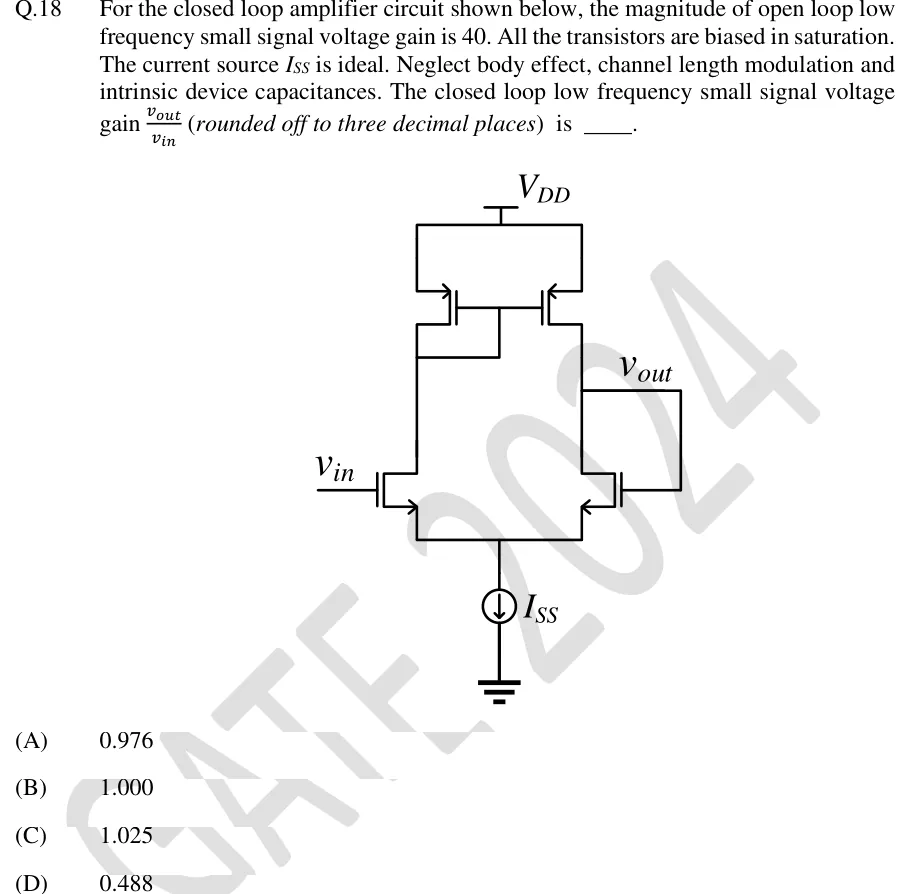
For the closed loop amplifier circuit shown below, the magnitude of open loop low frequency small signal voltage gain is 40. All the transistors are biased in saturation. The current source ISS is ideal. Neglect body effect, channel length modulation and intrinsic device capacitances. The closed loop low frequency small signal voltage gain vinvout (rounded off to three decimal places) is ____.
Tap to open full sizeFigure from the GATE 2024 EC paper. It is part of the question.Figure description
A five-transistor CMOS differential amplifier. Top rail V_DD. Two PMOS transistors, left and right, have their sources tied to V_DD and their gates tied together. The left PMOS is diode-connected: its gate is joined to its own drain. Below it, the drain of the left NMOS connects to that diode node. The left NMOS gate is driven by the input v_in. The drain of the right PMOS connects to the drain of the right NMOS, and this node is the output v_out. A wire runs from the v_out node down to the gate of the right NMOS, so the output drives that gate directly. The sources of both NMOS transistors are joined at a common node, which goes to ground through an ideal current source I_SS (arrow pointing down, towards ground).
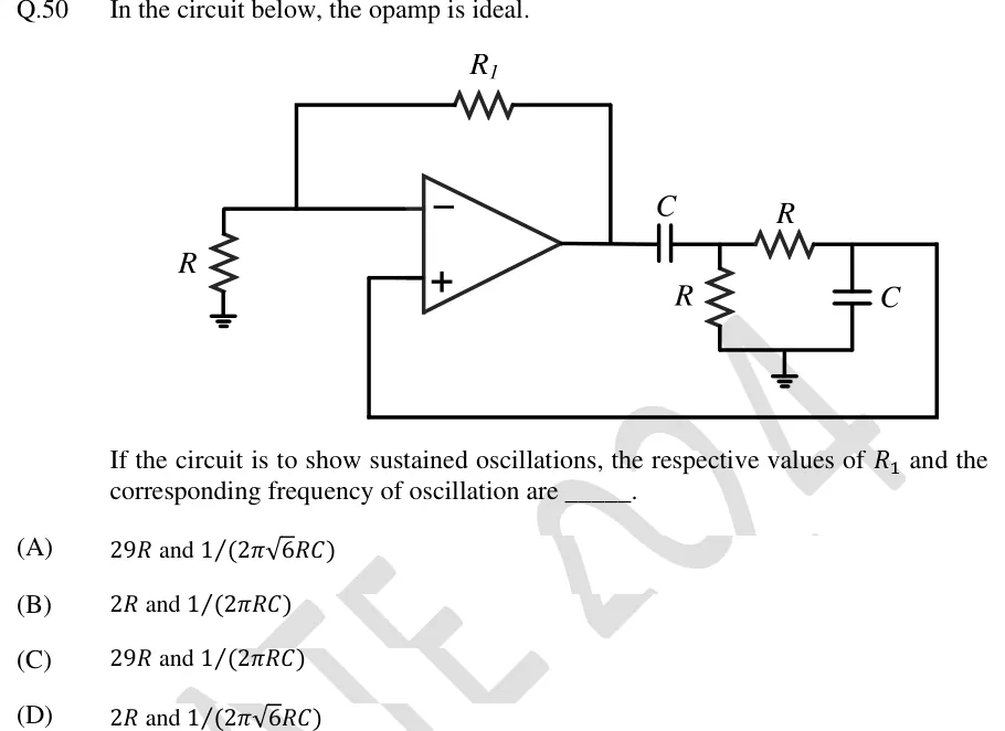
If the circuit is to show sustained oscillations, the respective values of R1 and the corresponding frequency of oscillation are _____.
Tap to open full sizeFigure from the GATE 2024 EC paper. It is part of the question.Figure description
An op-amp with its inverting (-) input on top and non-inverting (+) input below. The inverting input goes to ground through a resistor R, and a feedback resistor R_1 connects the inverting input to the op-amp output. So the op-amp is a non-inverting amplifier with gain 1 + R_1/R. From the output, a series capacitor C goes to node A. A resistor R connects node A to ground. A series resistor R goes from node A to node B. A capacitor C connects node B to ground. Node B is wired back along the bottom of the drawing to the non-inverting (+) input of the op-amp. The feedback network is therefore series C, shunt R, series R, shunt C (a high-pass CR section followed by a low-pass RC section). The ideal op-amp's + input draws no current, so node B is unloaded.
A negative-feedback amplifier has β=0.02 and open-loop gain A=5000. Through ageing, A falls by 20% to 4000 while β is unchanged. What is the resulting percentage decrease in the closed-loop gain, rounded to two decimal places?
▸ Answer and solution
Answer:0.25 (accepted range ±0.01)
Before: 1+Aβ=1+5000×0.02=101, so Af=5000/101=49.505.
After: 1+Aβ=1+4000×0.02=81, so Af=4000/81=49.383.
The differential formula would give 20%/101=0.198%. It underestimates here because a 20% change is not small.
PRACTICE 21 mark · NAT
An op-amp square-wave generator has R=10kΩ and C=0.1μF in its timing network (from the output to the inverting input, and from the inverting input to ground), and equal resistors R1=R2 in the divider that feeds the output back to the non-inverting input. The op-amp is ideal and saturates symmetrically at ±Vsat. What is the output frequency, in Hz, rounded to the nearest integer?
▸ Answer and solution
Answer:455 (accepted range ±2)
β=R1/(R1+R2)=1/2, and RC=104×10−7=1ms.
T=2RCln1−β1+β=2×1ms×ln3=2×1.0986ms=2.197ms.
f=1/T=1/(2.197×10−3)≈455Hz.
PRACTICE 31 mark · MCQ
A single-stage BJT common-emitter amplifier has an emitter resistor RE that is not bypassed. The signal is applied at the base and the output is taken at the collector, and the transistor's finite output resistance ro is included. Treating RE as the feedback network, what are the feedback topology and its effect on the input resistance (looking into the base) and the output resistance (looking into the collector, excluding RC)?
Output side: the collector current ic≈ie flows through RE, so vf=ieRE is proportional to the output current. Opening the output loop (io=0) removes vf, so the sampling is current (series) sampling.
Input side: vf appears at the emitter, so around the input loop vbe=vs−vf. The feedback voltage is in series with the source, so the mixing is series mixing.
Series-series: series mixing raises Rin (to about rπ+(1+hfe)RE looking into the base), and current sampling raises the resistance looking into the collector from ro to about ro[1+gm(RE∥rπ)] with the base driven from a zero-resistance source.
Answer: (A).
PRACTICE 41 mark · NAT
An amplifier has a mid-band gain of 1000 and a single high-frequency pole at 50 kHz. Frequency-independent negative feedback is applied, which reduces the mid-band gain to 25. What is the upper 3-dB frequency of the feedback amplifier, in MHz?
▸ Answer and solution
Answer:2 (accepted range ±0.02)
1+AMβ=AM/AMf=1000/25=40.
Single pole: fHf=fH(1+AMβ)=50kHz×40=2MHz.
Check: the gain-bandwidth product is unchanged, 1000×50kHz=25×2MHz=50MHz.
PRACTICE 52 marks · MSQ
Which of the following statements is/are correct? Op-amps are ideal, and each oscillator is in steady state.
(A)
An op-amp RC phase-shift oscillator built with three identical high-pass sections (series C, shunt R), whose last resistor returns to the op-amp's virtual ground, oscillates at f0=1/(2π6RC) and needs an inverting gain of magnitude at least 29.
(B)
A Colpitts oscillator with C1=C2=C and inductor L oscillates at f0=1/(2π2LC).
(C)
An ideal quartz crystal (motional arm L,Cs, shunt capacitance Cp, resistance neglected) has an inductive reactance at frequencies between its series and parallel resonant frequencies.
(D)
A Wien-bridge oscillator with equal resistors R and equal capacitors C needs a non-inverting amplifier gain of at least 29.
▸ Answer and solution
Answer: (A), (C)
(A) True. For three identical high-pass sections, β=1/[(1−5α2)−j(6α−α3)] with α=1/(ωRC). The imaginary part vanishes at α2=6, which gives f0=1/(2π6RC) and β=1/(1−30)=−1/29, so ∣A∣≥29.
(B) False. Ceq=C⋅C/(2C)=C/2, so f0=1/(2πLC/2)=2/(2πLC), not 1/(2π2LC).
(C) True. X=−(ω2−ωs2)/[ωCp(ω2−ωp2)] is positive (inductive) for ωs<ω<ωp.
(D) False. With equal components the Wien network gives β=1/3 at f0=1/(2πRC), so the amplifier needs A≥3.
Answer: (A) and (C).
PRACTICE 62 marks · MCQ
A Wien-bridge feedback network has a series arm of R in series with C and a shunt arm of R in parallel with 2C. Its output is taken across the shunt arm, and it drives an ideal non-inverting amplifier of gain 1+Rf/Rg (infinite input resistance, zero output resistance). What are the oscillation frequency ω0 and the minimum amplifier gain?
(A)
ω0=2RC1, minimum gain 4
(B)
ω0=2RC1, minimum gain 3
(C)
ω0=RC2, minimum gain 4
(D)
ω0=RC1, minimum gain 3.5
▸ Answer and solution
Answer: (A)
With R1=R2=R,C1=C (series arm) and C2=2C (shunt arm): β=Zs+ZpZp=1+s(R1C1+R2C2+R2C1)+s2R1R2C1C2sC1R2.
The phase is zero when the real part of the denominator vanishes: ω02R1R2C1C2=1, so ω0=1/R2⋅2C2=1/(2RC).
At ω0:β=R1C1+R2C2+R2C1R2C1=1+R1/R2+C2/C11=1+1+21=41.
Barkhausen: Aβ=1 needs A≥4, i.e. Rf≥3Rg. Answer: (A).

 Tap to open full size