
IAE Academy

GATE 2024 EC Q.18: solution and answer

GATE 2024 · ECQ.18 · 1 mark · MCQ

For the closed loop amplifier circuit shown below, the magnitude of open loop low frequency small signal voltage gain is 40. All the transistors are biased in saturation. The current source is ideal. Neglect body effect, channel length modulation and intrinsic device capacitances. The closed loop low frequency small signal voltage gain (rounded off to three decimal places) is ____.
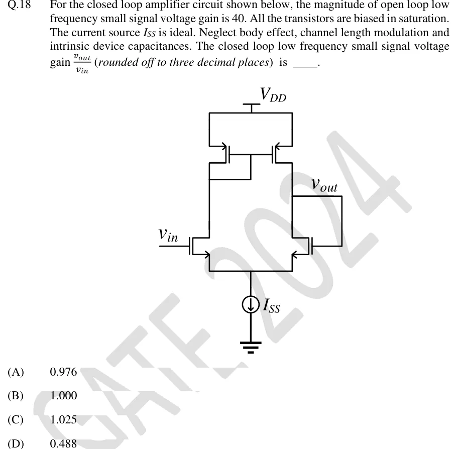
GATE 2024 EC question 18: A five-transistor CMOS differential amplifier.Tap to open full size
Figure from the GATE 2024 EC paper. It is part of the question.
Figure description

A five-transistor CMOS differential amplifier. Top rail V_DD. Two PMOS transistors, left and right, have their sources tied to V_DD and their gates tied together. The left PMOS is diode-connected: its gate is joined to its own drain. Below it, the drain of the left NMOS connects to that diode node. The left NMOS gate is driven by the input v_in. The drain of the right PMOS connects to the drain of the right NMOS, and this node is the output v_out. A wire runs from the v_out node down to the gate of the right NMOS, so the output drives that gate directly. The sources of both NMOS transistors are joined at a common node, which goes to ground through an ideal current source I_SS (arrow pointing down, towards ground).

  1. (A)

    0.976

  2. (B)

    1.000

  3. (C)

    1.025

  4. (D)

    0.488

Answer and solution

ANSWER

The closed-loop gain is , so the answer is option (A).

Official answer: ASource: Official answer key, GATE 2024 EC (IISc Bengaluru)

  1. Identify the circuit. This is the standard five-transistor OTA. It has an NMOS differential pair, (left) and (right), a PMOS current-mirror load, (left, diode-connected) and (right), and an ideal tail source . The output is taken at the common drain node of and .

  2. Find the input polarity. Raise the gate voltage of . Then increases, and because the tail current is fixed, falls by the same amount. The mirror copies the increase in through into the output node, while draws less current out of it. So rises. The gate of is therefore the non-inverting input and the gate of is the inverting input .

  3. Open-loop model. The tail source is ideal, so a common-mode change on the two gates cannot change the drain currents, and the output responds only to the difference between the gates: . The question gives the open-loop low-frequency gain as , so no device-level calculation is needed.

  4. Identify the feedback. The output is wired straight to the gate of , so and . A MOSFET gate draws no current, so this wire does not load the output. The whole output is fed back to the inverting input, which is negative feedback with and a loop gain of . The circuit is a unity-gain buffer built with a finite-gain amplifier.

  5. Closed-loop gain.

  6. Evaluate. , which is option (A). The gain falls just short of 1 because the loop gain is finite. The fractional error is .

KEY IDEA

The output of the five-transistor OTA is tied straight to its inverting input, the gate of . That makes it a unity-gain buffer with . With a finite open-loop gain , the closed-loop gain is , not exactly 1.

WATCH OUT FOR

Answering 1.000 by treating the buffer as ideal, which assumes infinite open-loop gain. Other traps: halving the gain as if the single-ended output of a differential pair gave half, which leads to 0.488; getting the feedback sign wrong or using , which leads to about 1.025. Check the polarity first. The gate of is the inverting input, so the feedback is negative and the gain is .

From the GATE 2024 EC paper. Every question of this paper · Download the full paper · All 4 Feedback & oscillators questions, with notes

More Feedback & oscillators questions