
IAE Academy

GATE 2023 EC Q.21: solution and answer

GATE 2023 · ECQ.21 · 1 mark · MCQ

In the circuit shown below, and are bias voltages. Based on input and output impedances, the circuit behaves as a
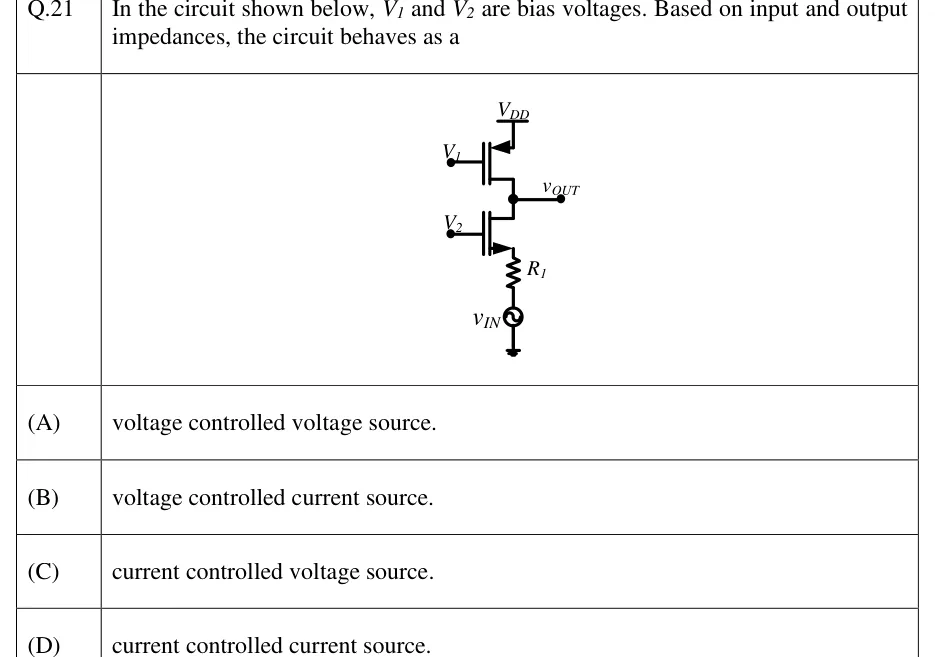
GATE 2023 EC question 21: Two MOSFETs are stacked in series between V_DD and the input source.Tap to open full size
Figure from the GATE 2023 EC paper. It is part of the question.
Figure description

Two MOSFETs are stacked in series between V_DD and the input source. Top device: a PMOS whose source is connected to V_DD (the source arrow points into the device) and whose gate is driven by the DC bias V_1. Its drain goes to the output node, marked v_OUT. Bottom device: an NMOS whose gate is driven by the DC bias V_2 and whose drain is connected to the same output node v_OUT. Its source (the arrow points out) connects to one end of a resistor R_1. The other end of R_1 goes to the top terminal of an AC voltage source v_IN (a circle with a tilde, no polarity marks), whose bottom terminal is grounded. So v_IN, through the series resistor R_1, drives the NMOS source, and the output is taken at the common drain node of the NMOS and the PMOS.

  1. (A)

    voltage controlled voltage source.

  2. (B)

    voltage controlled current source.

  3. (C)

    current controlled voltage source.

  4. (D)

    current controlled current source.

Answer and solution

ANSWER

The circuit is a common-gate stage with an active PMOS load. Its input resistance is low (about ), its output resistance is high (about ) and its current gain is unity, so it behaves as a current-controlled current source, option (D).

Official answer: DSource: Official answer key, GATE 2023 EC (IIT Kanpur)

  1. Identify the devices. The top PMOS has its source at and its gate at the DC bias . Both are AC ground, so it has no small-signal drive. Seen from its drain, it is just its output resistance , an active (current-source) load. The bottom NMOS has its gate at the DC bias , so its gate is at AC ground. The signal enters at its source and leaves at its drain, so the NMOS is a common-gate stage. The source in series with is the signal source together with its own resistance. Its Norton equivalent is a current in parallel with . So the amplifier's input port is the NMOS source and its output port is the drain node .

  2. Small-signal model and assumptions. Each MOSFET is modelled as with from drain to source. Body effect is neglected, and we take . The NMOS gate is at AC ground, so .

  3. Input resistance, looking into the NMOS source. Apply a test voltage at the source and let flow in. The gate draws no current, so leaves through the drain into , which gives . The current through the NMOS from source to drain is Solving for : With comparable to , . That is of the order of , so the input impedance is low.

  4. Output resistance, looking into the drain node. Set , so the NMOS source goes to ground through . Apply at the drain and let flow into the NMOS drain. Then and , so Looking up, you see the PMOS resistance . So This is of the order of , so the output impedance is high.

  5. Transfer. The gate draws no current, so the current entering the NMOS source is exactly the current leaving its drain: . is much smaller than the source resistance , so almost all of the Norton current goes into the source: . With the output shorted to AC ground, carries no current and . The short-circuit current gain is , so the stage is a current buffer.

  6. Classify. Each ideal controlled source has fixed port impedances. VCVS: , . VCCS: , . CCVS: , . CCCS: , . This circuit has a low (about ) and a high (about ), which matches the current-controlled current source, option (D).

KEY IDEA

Classify an amplifier by its port impedances. A low input impedance means it takes a current in, and a high output impedance means it delivers a current. A common-gate MOSFET has at the source, of the order of at the drain, and , so it is a current buffer, which is a CCCS.

WATCH OUT FOR

Students often classify from the labels instead of the impedances. Because the input is drawn as a voltage and the output is labelled , they pick VCVS, or VCCS by thinking of a transconductance stage. Others count as part of the amplifier's input impedance. belongs to the driving source (Norton current ), and the amplifier's own input, the NMOS source, has an impedance of only about . A third error is to read the NMOS as a source follower, which would give low output impedance. Its gate is at AC ground and the output is at its drain, so it is common-gate.

From the GATE 2023 EC paper. Every question of this paper · Download the full paper · All 20 Amplifiers questions, with notes

More Amplifiers questions