
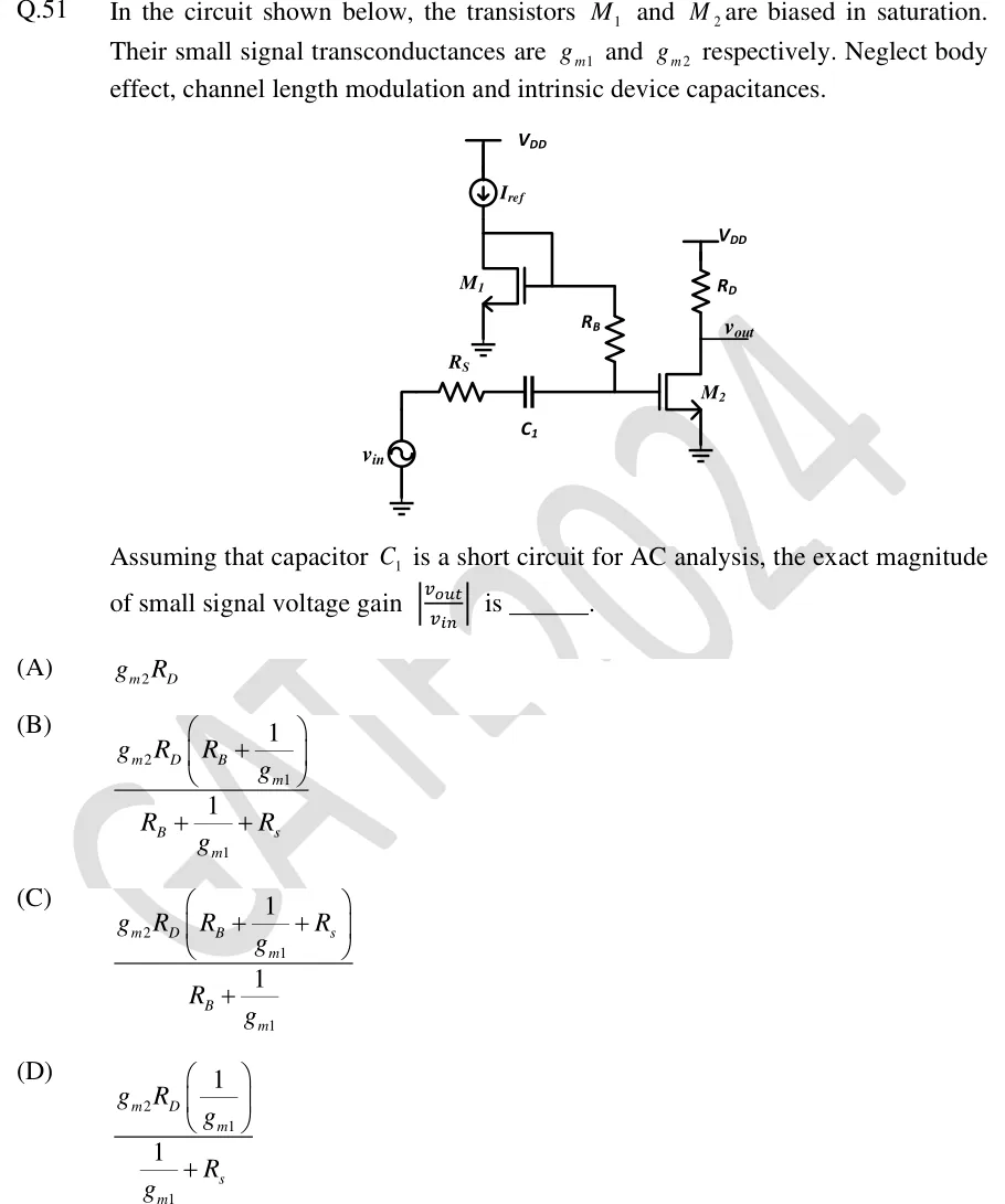
In the circuit shown below, the transistors and are biased in saturation. Their small signal transconductances are and respectively. Neglect body effect, channel length modulation and intrinsic device capacitances.
[Figure]
Assuming that capacitor is a short circuit for AC analysis, the exact magnitude of small signal voltage gain is ______.
 Tap to open full size
Figure description
Two NMOS transistors. Left branch: a current source I_ref (arrow pointing down) from V_DD feeds the drain of NMOS M_1; the source of M_1 is grounded. The drain of M_1 is tied by a wire to the gate of M_1 (diode-connected), and this same drain/gate node connects to the top of resistor R_B. The bottom of R_B goes to the gate of NMOS M_2. Input: an AC source v_in (bottom terminal grounded) in series with resistor R_S and capacitor C_1, the far side of C_1 connected to the gate of M_2 (same node as the bottom of R_B). Right branch: M_2 source grounded, drain connected through R_D to V_DD; the output v_out is taken at the drain of M_2.
- (A)
- (B)
- (C)
- (D)