
IAE Academy

GATE 2022 IN Q.47: solution and answer

GATE 2022 · INQ.47 · 2 marks · MCQ

In the small signal circuit shown, the enhancement mode n-channel MOSFET is biased in saturation with a transconductance . A small signal low-frequency voltage injected at the supply terminal results in a small signal voltage fluctuation at the output. If the channel length modulation of the MOSFET is ignored, the small signal gain is given by ________
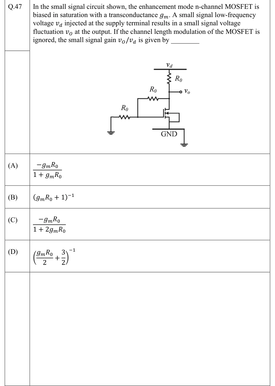
GATE 2022 IN question 47: Small-signal circuit with one enhancement-mode n-channel MOSFET (body arrow pointing into the channel;Tap to open full size
Figure from the GATE 2022 IN paper. It is part of the question.
Figure description

Small-signal circuit with one enhancement-mode n-channel MOSFET (body arrow pointing into the channel; body tied to the source). A horizontal supply rail at the top is labelled v_d. A resistor R_0 runs from the v_d rail down to the drain node. The drain node is also the output terminal v_o (open circle to the right). A second resistor R_0 runs from the drain node across to the gate node (drain-to-gate feedback resistor). A third resistor R_0 runs from the gate node to ground (ground symbol at the left). The source, together with the body, connects to the bottom rail labelled GND, which is grounded. All three resistors are equal, R_0.

  1. (A)

  2. (B)

  3. (C)

  4. (D)

Answer and solution

ANSWER

The answer is (D): .

Official answer: DSource: Official answer key, GATE 2022 IN (IIT Kharagpur)

  1. Small-signal model: the MOSFET is replaced by a voltage-controlled current source flowing from drain to source. Channel-length modulation is ignored, so and there is no resistor in parallel with that source. The source is grounded, so , and the gate draws no current.

  2. Voltage divider at the gate: no current flows into the gate, so the drain-to-gate and the gate-to-ground carry the same current. They form a divider from the output node to ground:

  3. KCL at the drain (output) node. The current coming down from the supply through the top equals the channel current plus the current into the feedback divider, which is from to ground:

  4. Collect the terms:

  5. Therefore

  6. Cross-check by impedances. Since , the transistor draws from the output node, so it behaves like a resistance from output to ground. That resistance is in parallel with the divider: The output is then a plain divider of against : This agrees with the KCL result.

  7. Checking the options. With the circuit is just in series with , so . Option (D) gives , but (B) gives . The gain is also positive (a divider with a passive load), which rules out (A) and (C), both of which are negative. The answer is (D).

KEY IDEA

The gate draws no current, so the two lower resistors form a divider and . The MOSFET therefore loads the output like a resistance to ground, in parallel with . The supply fluctuation reaches the output through a divider of against .

WATCH OUT FOR

There are two common mistakes. The first is to take , forgetting the gate divider, and also leave out the current in the feedback path. KCL then reduces to , which gives , the trap option (B). The second is to treat the circuit as a common-source amplifier driven at the gate, which gives an inverting gain like (A) or (C). Here the signal enters at the supply, not the gate, and the gain is positive and below 1.

From the GATE 2022 IN paper. Every question of this paper · Download the full paper · All 20 Amplifiers questions, with notes

More Amplifiers questions