
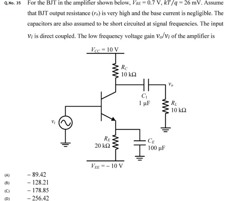
For the BJT in the amplifier shown below, , . Assume that BJT output resistance () is very high and the base current is negligible. The capacitors are also assumed to be short circuited at signal frequencies. The input is direct coupled. The low frequency voltage gain of the amplifier is
 Tap to open full size
Figure description
Common-emitter amplifier with an NPN BJT and split supplies. The collector connects through R_C = 10 k Ω to V_CC = 10 V. The emitter (arrow pointing out, NPN) connects through R_E = 20 k Ω to V_EE = -10 V; a bypass capacitor C_E = 100 connects from the emitter to ground. The base is driven directly (no coupling capacitor, no bias resistors) by an AC source v_i whose other terminal is grounded. The collector is coupled through C_1 = 1 to the output node v_o, which is loaded by R_L = 10 k Ω to ground.
- (A)
- (B)
- (C)
- (D)