
IAE Academy

GATE 2026 EC Q.50: solution and answer

GATE 2026 · ECQ.50 · 2 marks · MCQ

A small signal source, is applied to a BJT circuit as shown in the Figure.

Assume zero source resistance, V, , Early voltage V and Thermal voltage mV. Effect of internal parasitic capacitances of the BJT may be neglected.

Which expression is the best approximation of the output voltage ?
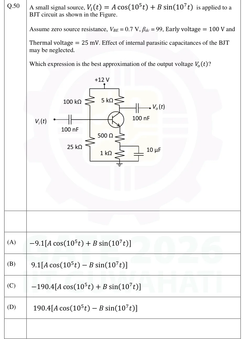
GATE 2026 EC question 50: Single-stage common-emitter amplifier with an NPN BJT.Tap to open full size
Figure from the GATE 2026 EC paper. It is part of the question.
Figure description

Single-stage common-emitter amplifier with an NPN BJT. Supply rail +12 V at the top. Base bias divider: 100 kΩ from +12 V to the base node, 25 kΩ from the base node to ground. The source V_i(t) connects to the base node through a series 100 nF coupling capacitor. Collector: 5 kΩ from +12 V to the collector. The output V_o(t) is taken from the collector through a series 100 nF coupling capacitor, with no load resistor shown (open output terminal). Emitter: 500 Ω from the emitter to an intermediate node, then 1 kΩ from that node to ground. A 10 µF capacitor is connected from the intermediate node (junction of 500 Ω and 1 kΩ) to ground, so it bypasses only the 1 kΩ resistor. The bottom of the 25 kΩ, the 1 kΩ and the 10 µF share the ground.

  1. (A)

  2. (B)

  3. (C)

  4. (D)

Answer and solution

ANSWER

Both tones fall in the mid-band. The coupling and bypass reactances are negligible and the BJT's parasitic capacitances are neglected, so both tones see the same inverting gain of a CE stage degenerated by the unbypassed 500 Ω, . That gives , option (A).

Official answer: ASource: Official answer key, GATE 2026 EC (IIT Guwahati)

  1. DC bias (all capacitors open). Replace the base divider with its Thevenin equivalent: and . With the 10 µF capacitor open, the DC current flows through both emitter resistors, so .

  2. KVL around the base-emitter loop: so (the Early effect is ignored for the bias point) and . Check the region: and , so . The transistor is in the active region.

  3. Small-signal parameters (hybrid- model, taking ): , , . In the model, sits between base and emitter, and the source and both run from collector to emitter. The BJT's parasitic capacitances are left out, as the question says.

  4. Capacitor reactances at the lower tone, : and . At both are 100 times smaller: and .

  5. Both tones are in the mid-band. Input: . The source resistance is zero, so the input capacitor and form a divider: , with a phase lead of at and less at . Output: there is no load, so no signal current flows through the output capacitor and at both frequencies. Emitter: the 1 kΩ in parallel with 10 µF has an impedance of about at ( at ). That is negligible next to the 500 Ω in series with it, so the AC emitter resistance is . High frequencies: the parasitic capacitances are neglected, so the gain does not roll off. Both tones therefore see the same real, inverting gain.

  6. Mid-band gain of a CE stage with an unbypassed . The standard approximation takes and treats as if it were in parallel with : Cross-check without those approximations. With neglected, the model gives exactly . Putting back where it really is (collector to emitter) moves this only to about : the emitter degeneration raises the resistance seen looking into the collector to about , far above . Every model gives a gain of about . None comes near 190.

  7. Output: the same real gain multiplies both components, so Option (A) is the only option with a magnitude near 9 and the same inverting sign on both terms.

  8. Why not the others: (printed as 190.4 in (C) and (D)) would be the gain only if the whole emitter resistance were bypassed. Here the 500 Ω is not bypassed, so (C) is out. Options (B) and (D) make the term non-inverting and flip the sign of only the term. A CE stage inverts, and a phase difference between two tones that both sit in the flat mid-band is impossible.

KEY IDEA

Bias with the full 1.5 kΩ in the emitter ( mA, so mS). Then check that both tones are in the mid-band: at rad/s the 100 nF capacitors are 100 Ω, which is tiny next to a 14.5 kΩ input and an open output, and the 10 µF is 1 Ω, which leaves only the 500 Ω unbypassed. With the parasitics neglected, both tones see one real gain, .

WATCH OUT FOR

Treating the emitter as fully bypassed and taking the gain as (option C). The 10 µF bypasses only the 1 kΩ, so the 500 Ω still degenerates the gain by a factor of . Another trap is assuming the rad/s tone picks up a different phase and flips sign (options B and D). With the parasitics neglected and the coupling capacitors already short at rad/s, both tones sit in the flat mid-band. Also watch the bias: the DC emitter resistance is the full 1.5 kΩ, not 500 Ω.

From the GATE 2026 EC paper. Every question of this paper · Download the full paper · All 20 Amplifiers questions, with notes

More Amplifiers questions