
IAE Academy

ISRO EC 2025 Q.46: solution and answer

ISRO 2025 · ECQ.46 · 1 mark · MCQ

In the below figure, determine the signs on the OPAMP terminals A and B for negative feedback operation and gate potential of the transistor for Vref = 3V and Vdd = 5V. , .
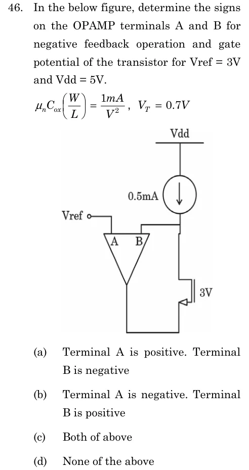
ISRO EC 2025 question 46: A supply rail Vdd at the top.Tap to open full size
Figure from the ISRO EC 2025 paper. It is part of the question.
Figure description

A supply rail Vdd at the top. Below it, an ideal 0.5 mA current source (circle with a downward arrow) feeds current down into a node. That node connects to the drain of an n-channel MOSFET below it, and also by a wire to op-amp input terminal B. The MOSFET gate is labelled 3V (fixed gate voltage). The MOSFET source (arrow terminal) is connected by a wire to the op-amp output at the bottom tip of the triangle. Op-amp terminal A (left input) is connected to Vref. The op-amp triangle points downward with A on the left and B on the right; the signs on A and B are not marked in the figure.

  1. (A)

    Terminal A is positive. Terminal B is negative

  2. (B)

    Terminal A is negative. Terminal B is positive

  3. (C)

    Both of above

  4. (D)

    None of the above

Answer and solution

ANSWER

Terminal A is positive (non-inverting) and terminal B is negative (inverting), option (a). The gate sits at .

Official answer: ASource: ISRO's final answer key of 15 May 2026

  1. Read the circuit. The current source pushes current down into a node. That node is the MOSFET drain and is also wired to terminal B. The MOSFET gate is fixed at . The MOSFET source is wired to the op-amp output. is applied to terminal A.

  2. Find the sign of B by tracing the loop. Suppose the output rises. The source voltage rises, so falls and the MOSFET can carry less current.

  3. The current source still supplies , but the transistor now takes less. The surplus current charges the drain node, so the drain voltage, which is , rises.

  4. A rise in the output therefore raises . For negative feedback, a rise in the output must push the output back down, so B must be the inverting (negative) terminal. Terminal A is then the non-inverting (positive) terminal.

  5. Check the operating point, assuming saturation: , so . This gives , so .

  6. With the virtual short, , so the drain is at . The source is at , giving . Since and , the MOSFET is in saturation, as assumed. The gate potential is .

  7. So A is positive and B is negative, which is option (a). Option (b) would be the positive-feedback connection, so options (c) and (d) are also wrong.

KEY IDEA

To find which op-amp input is inverting, raise the output and follow the loop through the circuit. The input that rises with the output must be the inverting one. Here a higher output lowers , so the transistor current falls and the drain node (terminal B) rises.

WATCH OUT FOR

Assuming the input connected to the transistor side is the non-inverting one without tracing the loop. Here the output drives the source, not the gate, so the usual common-source inversion does not apply and the sign comes out opposite to a quick guess.

From the ISRO EC 2025 paper. Every question of this paper · The full paper (PDF, ISRO) · All 4 ISRO Op-amps questions, with notes

More ISRO Op-amps questions