GATE 2026 EC Q.27
A binary ripple counter is designed to count to .
Which of the following is/are the number of flip-flops required to design the counter?
- (A)
6
- (B)
7
- (C)
4
- (D)
5

GATE EC · EE · IN
Flip-flops, counters, shift registers, state machines and timing
Sequential circuits have memory: their outputs depend on stored state as well as on the present inputs, and in a synchronous circuit flip-flops update that state at clock edges. The standard problems are tracing a counter or shift register clock by clock, analysing or converting flip-flops with their characteristic and excitation tables, drawing the state diagram of a sequence detector, finding the maximum clock frequency or checking hold time from delay data, and finding the timing of a 555 timer. Each is mechanical once the tables, formulas and timing inequalities below are learned.
30 previous-year questions · 30 solved · 5 practice questions
Conventions in these notes. A complement is written with an overline, so means NOT . is the present state (just before the active clock edge) and is the next state (just after it). Positive logic is used (1 = HIGH). Flip-flops are positive-edge-triggered unless stated otherwise. A multi-bit state such as is written MSB first. X in a table means don't care. The propagation delay of a flip-flop, , is its clock-to-Q delay . Setup time and hold time are defined in the timing section.
A combinational circuit's output depends only on its present inputs. A sequential circuit's output also depends on stored state. The basic storage element is the SR latch. It is built either from two cross-coupled NOR gates with active-HIGH inputs and , or from two cross-coupled NAND gates with active-LOW inputs and .
NOR latch: S R | NOR latch: | NAND latch: | NAND latch: |
|---|---|---|---|
0 0 | (hold) | 1 1 | (hold) |
0 1 | 0 (reset) | 1 0 | 0 (reset) |
1 0 | 1 (set) | 0 1 | 1 (set) |
1 1 | Forbidden: | 0 0 | Forbidden: |
Why S = R = 1 is forbidden in the NOR latch. Both outputs are forced to 0, so and are no longer complements of each other. It gets worse if and then return to 0 together: the two gates race, and the final state cannot be predicted. The NAND latch has the same fault when both of its active-LOW inputs are 0, which forces both outputs to 1.
Gated latches. A gated (clocked) SR latch adds an enable input EN. With EN = 0 it holds its state whatever and do. With EN = 1 it behaves as an SR latch, so with EN = 1 is still forbidden. The gated D latch connects and , which removes the forbidden input. While EN = 1 the output follows (the latch is transparent), and when EN goes to 0 the latch holds the last value of .
Property | Gated latch | Edge-triggered flip-flop |
|---|---|---|
Responds to | The level of the enable (clock) | Only the active clock edge |
Output while the clock is active | Follows the input (transparent) | Held; changes once, just after the edge |
Edge-triggered and master-slave flip-flops. An edge-triggered flip-flop samples its inputs only at the active clock edge, so its state changes at most once per clock period. A master-slave flip-flop is two latches in series, enabled on opposite clock phases. In the usual arrangement the master is transparent while CLK = 1 and the slave while CLK = 0. The output therefore changes only when the clock falls. Apart from a brief overlap caused by the delay of the clock inverter, the two latches are never transparent at the same time.
Race-around condition. Consider a level-triggered JK flip-flop with . The output toggles, the new output feeds back to the input gates, and the output toggles again. This repeats for as long as the clock stays HIGH, so the state left after the pulse cannot be predicted. It happens when the clock pulse width is longer than the flip-flop's propagation delay . Master-slave and edge-triggered designs remove it. A level-triggered JK can avoid it only by keeping the clock pulse narrower than the propagation delay.
CONDITION TO AVOID RACE-AROUND
= width of the HIGH clock pulse, = flip-flop propagation delay, = clock period. Applies to a level-triggered JK flip-flop in toggle mode ().
EXAM TIP
In a waveform question, first check whether the element is a latch or an edge-triggered flip-flop. A D latch's output copies for as long as the enable is active. A D flip-flop copies only at the edge and ignores any change in between. The same and clock waveforms therefore give different outputs.
EXAM TIP
A master-slave JK cures race-around, but its master is open for the whole HIGH phase. A brief 1 on (when ) or on (when ) during that phase is therefore caught by the master and passed to the output at the falling edge, even if the input went back to 0 before the edge. This fault is called 1s catching. Edge-triggered flip-flops do not have it.
The characteristic table (or characteristic equation) gives the next state from the inputs and the present state . Use it to analyse a circuit. The excitation table answers the reverse question: which inputs produce a required transition ? Use it to design counters and state machines.
SR FLIP-FLOP
The constraint is part of the equation, because is not allowed. holds, sets, resets.
JK FLIP-FLOP
holds, resets, sets, toggles. No input combination is forbidden.
D FLIP-FLOP
The next state is the value of at the active edge, so a D flip-flop delays its input by one clock period.
T FLIP-FLOP
toggles, holds. In toggle mode the output frequency is half the clock frequency, and n toggling stages in cascade divide the clock by .
Action | |||
|---|---|---|---|
0 | 0 | Hold | |
0 | 1 | 0 | Reset |
1 | 0 | 1 | Set |
1 | 1 | Toggle |
Transition | S R | J K | D | T |
|---|---|---|---|---|
0 X | 0 X | 0 | 0 | |
1 0 | 1 X | 1 | 1 | |
0 1 | X 1 | 0 | 1 | |
X 0 | X 0 | 1 | 0 |
Write the characteristic table of the flip-flop you need (the target): its inputs and as columns, and as the result.
For every row, look up in the available flip-flop's excitation table the inputs it needs to make that transition.
Plot each input of the available flip-flop on a K-map whose variables are the target's inputs and . Use the X entries as don't cares.
Minimise. The resulting expressions are the gates placed in front of the available flip-flop.
Available flip-flop | Required behaviour | Input logic (Q = present output) |
|---|---|---|
JK | T | |
JK | D | , |
JK | SR | , (with ) |
D | T | |
D | JK | |
T | D | |
T | JK | |
SR | D | , |
SR | JK | , |
SR | T | , |
EXAM TIP
Two one-line shortcuts cover most conversions. To build any flip-flop from a D flip-flop, set equal to the target's characteristic equation (for JK, ). To build any flip-flop from a T flip-flop, set , so that T is 1 exactly when the output must change (for JK, ).
EXAM TIP
Asynchronous preset and clear inputs act immediately, without waiting for the clock, and override the synchronous inputs. They are often active-LOW (drawn with a bubble), so check for the bubble before tracing a circuit. Preset and clear must not be asserted together: as with in a latch, and stop being complements and the state left afterwards is unpredictable.
A counter steps through a fixed cycle of states, one step per clock pulse. A mod-N counter has N states in its cycle, so its state repeats every N clock pulses and it divides the clock frequency by N. With n flip-flops at most states exist, and any state outside the cycle is an unused state. A counter also works as a timer: counting pulses from a clock of known frequency measures time, since pulses take .
MINIMUM FLIP-FLOPS FOR N STATES
Applies to a mod-N counter and to an N-state machine with binary state encoding. The unused states must be checked for lock-out.
OUTPUT FREQUENCY OF A MOD-N COUNTER
is the rate at which the whole state repeats. In a binary mod-N counter it is also the frequency of the most significant output. Lower bits can repeat faster: in a mod-6 binary counter (0 to 5), still alternates 0, 1 on every clock, so its frequency is . The output need not have a 50% duty cycle; in a mod-5 binary counter the MSB is HIGH for 1 clock period in 5. A mod-M counter cascaded into a mod-N counter gives a mod- counter with . In a full n-bit binary (mod-) counter, bit ( for the LSB) has frequency and a 50% duty cycle.
Asynchronous (ripple) counter. Only the first flip-flop receives the external clock. Each later flip-flop is clocked by the output of the one before it, and every stage is in toggle mode (, or ). A change must pass down the chain one flip-flop at a time, so the delays add. Whether the circuit counts up or down depends on the triggering edge and on which output clocks the next stage:
Flip-flops trigger on | Next stage clocked from | Next stage clocked from |
|---|---|---|
Negative (falling) edge | Up counter | Down counter |
Positive (rising) edge | Down counter | Up counter |
MAXIMUM CLOCK FREQUENCY OF AN N-BIT RIPPLE COUNTER
The worst case is a transition in which all n stages change (for example 0111 to 1000 in a 4-bit up counter), which takes . The clock period must be at least this long for the count to settle, and be readable, before the next edge. If a decoder must also read the count, add its delay or strobe time : .
Mod-N ripple counter by reset. Connect every output that is 1 in the binary code of N to a NAND gate, and use it to drive the active-LOW asynchronous CLEAR of every flip-flop. Any number with all of these bits HIGH is at least N, so N is the first count that fires the gate. The count N lasts only a few nanoseconds before it is cleared (a transient state), so the stable sequence is 0 to . For a decade (mod-10) counter, , so the gate is a NAND of and . No count from 0 to 9 has both of these bits HIGH.
EXAM TIP
With an asynchronous CLEAR, decode the state N, because the clear acts immediately. With a synchronous CLEAR, which acts only at the next clock edge, decode instead. Decoding N there would give a mod- counter.
EXAM TIP
Decoding a ripple counter's outputs can produce false pulses. Going from 0111 to 1000, an up ripple counter passes briefly through 0110, 0100 and 0000 as each stage flips in turn. A synchronous counter avoids this sequence of false states, because all its stages switch on the same edge. Small differences between its flip-flops' delays can still produce much shorter spikes.
Synchronous counter. All flip-flops share the clock, so every stage that changes does so one clock-to-Q delay after the same edge. Combinational logic decides which stages change. In a binary up counter a bit toggles exactly when every lower bit is 1. In a down counter it toggles when every lower bit is 0.
SYNCHRONOUS BINARY COUNTER WITH T FLIP-FLOPS
This is the up counter. Down counter: . Up/down with mode input (1 = up, 0 = down): . With JK flip-flops, use .
Fix the count sequence and use flip-flops.
Write the state table: each present state with its next state. Unused states get don't-care next states.
From the chosen flip-flop's excitation table, write the input each flip-flop needs in every row. For D flip-flops, D is simply the next-state bit.
Minimise each input on a K-map of the present-state bits, using the unused states as don't cares.
Check for lock-out: work out where each unused state goes with the logic you chose. The counter is self-starting only if every unused state eventually enters the main cycle. If one does not, redesign with those next states fixed.
WORKED EXAMPLE
Design a synchronous counter with D flip-flops that counts (state , MSB first). Find minimal sum-of-products expressions for , and , using the unused states 110 and 111 as don't cares, and check whether the counter is self-starting.
Six states need flip-flops. For a D flip-flop, the required input is just the next value of that bit.
State table: , , , , , ; 110 and 111 are don't cares.
: the next is 1, 0, 1, 0, 1, 0 for present states 0 to 5, so .
: the next is 1 only for present states 001 and 010 (minterms 1 and 2); 6 and 7 are don't cares. Grouping 010 with 110 gives . State 001 has no adjacent 1 or X, so it stays as . Hence .
: the next is 1 for present states 011 and 100 (minterms 3 and 4); 6 and 7 are don't cares. Grouping 011 with 111 gives , and 100 with 110 gives . Hence .
Lock-out check. From 110: , , , so the next state is 111. From 111: , , , so the next state is 100, which is in the cycle.
Answer: , , . The counter is self-starting: .
The 555 timer. A timer can also be built around an RC circuit. The 555 timer IC contains two comparators, an SR flip-flop and a discharge transistor. With its control pin unused, the comparator thresholds are and . In astable mode (a free-running rectangular-wave oscillator) the timing capacitor charges through from to while the output is HIGH. It then discharges through alone, back to , while the output is LOW. In monostable mode (a one-shot) a trigger pulse, which takes the trigger pin below , sets the output HIGH. The output stays HIGH while charges through from 0 to , and then returns LOW.
555 ASTABLE MULTIVIBRATOR
: an RC charge toward from to , or a discharge toward 0 from to , takes . Duty cycle , which is always above 50% in this basic circuit. Applies to the standard astable connection with the control pin unused.
555 MONOSTABLE PULSE WIDTH
charges from 0 toward , and the output falls when reaches . So . Applies with the control pin unused.
A shift register is a chain of D flip-flops on a common clock, with each D input fed from the previous Q. The stored word moves one position per clock pulse, so an n-stage shift register also delays a serial bit stream by n clock periods, that is . Shift registers are classified by how data enter and leave:
Type | Data in | Data out | Clock pulses for an n-bit word |
|---|---|---|---|
SISO | Serial | Serial | n to load; the first bit fed in reaches the output after n clocks, the last after |
SIPO | Serial | Parallel | n, then all bits are read at once |
PISO | Parallel | Serial | 1 to load; the first bit is then at the output, and more shifts bring out the rest |
PIPO | Parallel | Parallel | 1 |
Shifting an unsigned binary number one place toward the MSB, with a 0 entering at the LSB, multiplies it by 2, provided no 1 is shifted out. Shifting it one place toward the LSB, with a 0 entering at the MSB, divides it by 2 and discards the remainder. For a signed number in 2's complement, a shift toward the LSB must copy the sign bit into the MSB (an arithmetic shift). It then divides by 2 and rounds toward : for example becomes . A universal (bidirectional) shift register has mode inputs that select hold, shift toward the MSB, shift toward the LSB, or parallel load.
Ring counter. The last flip-flop's Q feeds back to the first flip-flop's D, and the register is preset to a single 1 (for example 1000). The 1 circulates, giving n states with n flip-flops. No decoding is needed, because exactly one flip-flop is HIGH in each state.
Johnson counter (also called twisted-ring or switch-tail). The last flip-flop's feeds back to the first flip-flop's D. Starting from all zeros, the register fills with 1s from one end and then empties, giving 2n states with n flip-flops. Consecutive states differ in one bit, and each state can be decoded with a single 2-input gate. The 4-bit sequence, shifting from toward with , is:
Clock pulse | |
|---|---|
0 | 0000 |
1 | 1000 |
2 | 1100 |
3 | 1110 |
4 | 1111 |
5 | 0111 |
6 | 0011 |
7 | 0001 |
8 | 0000 (the cycle repeats) |
RING COUNTER WITH N FLIP-FLOPS (ONE CIRCULATING 1)
Each output is HIGH for one clock period in every n (duty cycle ). It is not self-starting without extra logic: from 0000, or from a state with two 1s, it never reaches the intended cycle.
JOHNSON COUNTER WITH N FLIP-FLOPS
Each output is a square wave with a 50% duty cycle. It is not self-starting without extra logic. In a 3-bit Johnson counter, for example, the unused states 010 and 101 switch back and forth between each other forever.
Linear feedback shift register (LFSR). If the first stage's D input is the XOR of selected flip-flop outputs, the all-zeros state maps to itself, because an XOR of 0s is 0. The longest cycle possible with n flip-flops is therefore states. Whether that maximum is reached depends on which outputs are fed back.
EXAM TIP
For N states, a binary counter needs flip-flops, a Johnson counter needs (N even) and a ring counter needs N. Ring and Johnson counters use more flip-flops in exchange for simple decoding.
EXAM TIP
Count clock pulses carefully in SISO questions. In an n-bit register, the first bit fed in appears at the serial output after n clocks, and the last bit of an n-bit word after clocks.
A finite state machine (FSM) is a synchronous sequential circuit with a finite set of states. Flip-flops hold the present state. Combinational next-state logic works out, from the present state and the inputs, the state to be loaded at the next clock edge. Combinational output logic produces the outputs. An FSM is specified by a state diagram or an equivalent state table.
Moore machine | Mealy machine | |
|---|---|---|
Output depends on | Present state only | Present state and present input |
In the state diagram | Output written inside each state | Output written on each transition, as input/output |
Output changes | Only after a clock edge | Also whenever the input changes (can glitch mid-period) |
Timing of a detection | One clock later: after the edge that enters the detecting state | In the same clock period as the last input bit |
States for the same task | Equal or more | Equal or fewer |
MINIMUM STATES TO DETECT ONE BIT PATTERN OF LENGTH L
Valid for both overlapping and non-overlapping detection. The states record how many pattern bits have been matched (0 to ), and a Moore machine needs one extra state whose output is 1. Minimum flip-flops = .
Overlapping and non-overlapping detection. With overlapping detection, the end of one occurrence can also be the start of the next: in 1011011 the pattern 1011 is found twice, sharing the middle 1. With non-overlapping detection the machine starts again from scratch after each detection, so 1011 is found only once in that string. The two state diagrams differ only in where the detecting transition goes. For overlapping detection it goes to the state for the longest proper suffix of the pattern (shorter than the whole pattern) that is also a prefix of it. For non-overlapping detection it goes to the reset state.
Create one state for each number of pattern bits matched so far: (none), (first bit), and so on. A Mealy machine stops at ; a Moore machine adds with output 1.
From each state, draw the transition for the correct next bit to the next state.
For the wrong bit, append it to the bits matched so far. Go to the state for the longest suffix of that string that is also a prefix of the pattern. This is not always .
For the detecting transition, go to the state for the longest proper suffix of the full pattern that is also a prefix of it (overlapping), or return to (non-overlapping). In a Moore machine the detecting transition enters , and the transitions out of are those of the state this rule names.
Check the diagram with a test string that contains overlaps.
Present state (bits matched) | : next state / | : next state / |
|---|---|---|
(none) | / 0 | / 0 |
(1) | / 0 | / 0 |
(10) | / 0 | / 0 |
(101) | / 0 | / 1 |
The table is a Mealy detector for 1011 with overlapping, with input and output . From with , the bits received end in 1010. The longest suffix of 1010 that is also a prefix of 1011 is 10, so the machine goes to , not . On detection ( in ), the longest proper suffix of 1011 that is also a prefix is 1, so the machine goes to ; a non-overlapping detector would go to instead. Trace for 1011011: () (), which is two detections. The Moore version needs a fifth state with output 1, and therefore 3 flip-flops instead of 2.
State minimisation. Two states are equivalent if every input sequence produces the same output sequence from both. Put another way: for each input they give the same output and move to equivalent next states. Equivalent states can be merged into one, which may reduce the number of flip-flops. Quick test: two rows of a state table with identical outputs and identical next-state entries are equivalent. Delete one row, rename its state to the other everywhere, and look again, because the renaming can make more rows identical. Complete method (partitioning): group the states by their output rows. Split any group whose members go to states in different groups for some input. Repeat until no group splits. Each final group is one state of the minimal machine.
EXAM TIP
A wrong bit does not always send a detector back to . Always ask which tail of the bits received so far could still be the start of the pattern.
EXAM TIP
A Mealy output can rise or glitch in the middle of a clock period when the input changes. If the output must stay clean for a whole period, pass it through a flip-flop. It then behaves like a Moore output, one clock later.
EXAM TIP
'Minimum number of flip-flops' for a state machine means binary encoding of the minimised machine, . One-hot encoding uses S flip-flops, with exactly one of them HIGH in each state.
Setup time : the data input must be stable for at least before the active clock edge.
Hold time : the data input must stay stable for at least after the active clock edge.
Clock-to-Q delay (the flip-flop propagation delay ): the time from the active edge until Q shows its new value. The maximum is used in the setup check, and the minimum (contamination delay) in the hold check.
Combinational delays: is the delay of the longest path through the logic between two flip-flops, and is the delay of the shortest path.
Violating setup or hold can make the flip-flop metastable: its output may sit between logic levels for an unpredictable time before settling.
Consider a launching flip-flop FF1 whose Q passes through combinational logic to the D input of a capturing flip-flop FF2. The setup check: data launched at one clock edge must reach FF2 at least before the next edge. The hold check: data launched at an edge must not reach FF2 until at least after that same edge has arrived at FF2, or it would overwrite the value FF2 is capturing. The critical path is the register-to-register path with the largest . With zero clock skew, that sum is the minimum clock period.
MAXIMUM CLOCK FREQUENCY (ZERO SKEW)
Follows from the setup constraint . Use the maximum clock-to-Q delay and the longest (critical) combinational path between any two flip-flops. Applies to synchronous counters, registers and FSMs.
HOLD CONSTRAINT (ZERO SKEW)
Uses the minimum (contamination) delays. The clock period does not appear, so slowing the clock cannot fix a hold violation. It is fixed by adding delay to the short path, or by using flip-flops with a shorter hold time or a longer minimum clock-to-Q delay.
Clock skew is the difference between the times at which the same clock edge arrives at different flip-flops. Sign convention used here: , the arrival time of the clock at FF2 minus its arrival time at FF1. Skew is positive when the capturing flip-flop receives the edge later.
SETUP CONSTRAINT WITH CLOCK SKEW
Positive skew gives the data extra time and relaxes setup; negative skew tightens it.
HOLD CONSTRAINT WITH CLOCK SKEW
Positive skew makes hold harder to meet; negative skew makes it easier. Skew therefore trades setup margin against hold margin.
WORKED EXAMPLE
Positive-edge-triggered flip-flop FF1 drives FF2 through combinational logic, and this is the only register-to-register path. For both flip-flops, is 1.0 ns (minimum) to 2.0 ns (maximum), ns and ns. The logic has ns and ns. (a) Find with zero skew, and check hold. (b) Repeat if the clock reaches FF2 1.0 ns later than FF1.
(a) Setup: ns, so MHz.
(a) Hold: ns ns, so hold is met with a 0.5 ns margin.
(b) ns. Setup: ns, so setup alone would allow MHz.
(b) Hold: we need ns. This fails by 0.5 ns, and no clock frequency fixes it. The shortest path must be lengthened by at least 0.5 ns (or the skew reduced by at least 0.5 ns), and the longest path must still meet setup afterwards.
Answer: (a) MHz, and hold is met with a 0.5 ns margin. (b) Setup allows 111.1 MHz, but hold is violated by 0.5 ns, so the circuit as drawn fails at every clock frequency.
EXAM TIP
An n-bit ripple counter needs , because the delays add along the chain. A synchronous counter needs only : one flip-flop delay however many bits it has, although the gate path may grow with n.
EXAM TIP
When Q is wired straight to D with no logic between stages, as in a shift register, . Setup then needs , and hold needs . Set when there is no skew.
EXAM TIP
In a counter or FSM, a flip-flop whose output returns through logic to its own input is also a register-to-register path, with zero skew. Include such paths when searching for the critical path.
EXAM TIP
If a question gives only one propagation delay for a flip-flop, use it as both the maximum and the minimum clock-to-Q delay.
PREVIOUS-YEAR QUESTIONS
Try each question first, then open the answer. We placed each question under a topic ourselves; the exam paper does not label topics.
See these papers in full: GATE ECE 2026 · GATE ECE 2025 · GATE ECE 2024 · GATE ECE 2023 · GATE ECE 2022 · GATE ECE 2020 · GATE ECE 2018 · GATE EE 2024 · GATE EE 2023 · GATE EE 2022 · GATE EE 2020 · GATE EE 2018 · GATE IN 2026 · GATE IN 2025 · GATE IN 2024 · GATE IN 2023 · GATE IN 2022 · GATE IN 2020 · GATE IN 2018
A binary ripple counter is designed to count to .
Which of the following is/are the number of flip-flops required to design the counter?
6
7
4
5
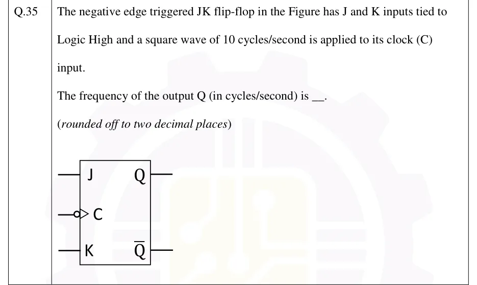
The negative edge triggered JK flip-flop in the Figure has J and K inputs tied to Logic High and a square wave of 10 cycles/second is applied to its clock (C) input.
The frequency of the output Q (in cycles/second) is ____. (rounded off to two decimal places)
 Tap to open full size
A single JK flip-flop drawn as a rectangle. Inputs on the left side: J (top), clock input C (middle) drawn with a bubble followed by the triangle clock symbol, marking negative-edge triggering, and K (bottom). Outputs on the right side: Q (top) and Q-bar (bottom). Each terminal is a short line with no further connections drawn. The text says J and K are tied to logic High and a 10 cycles/second square wave drives C.
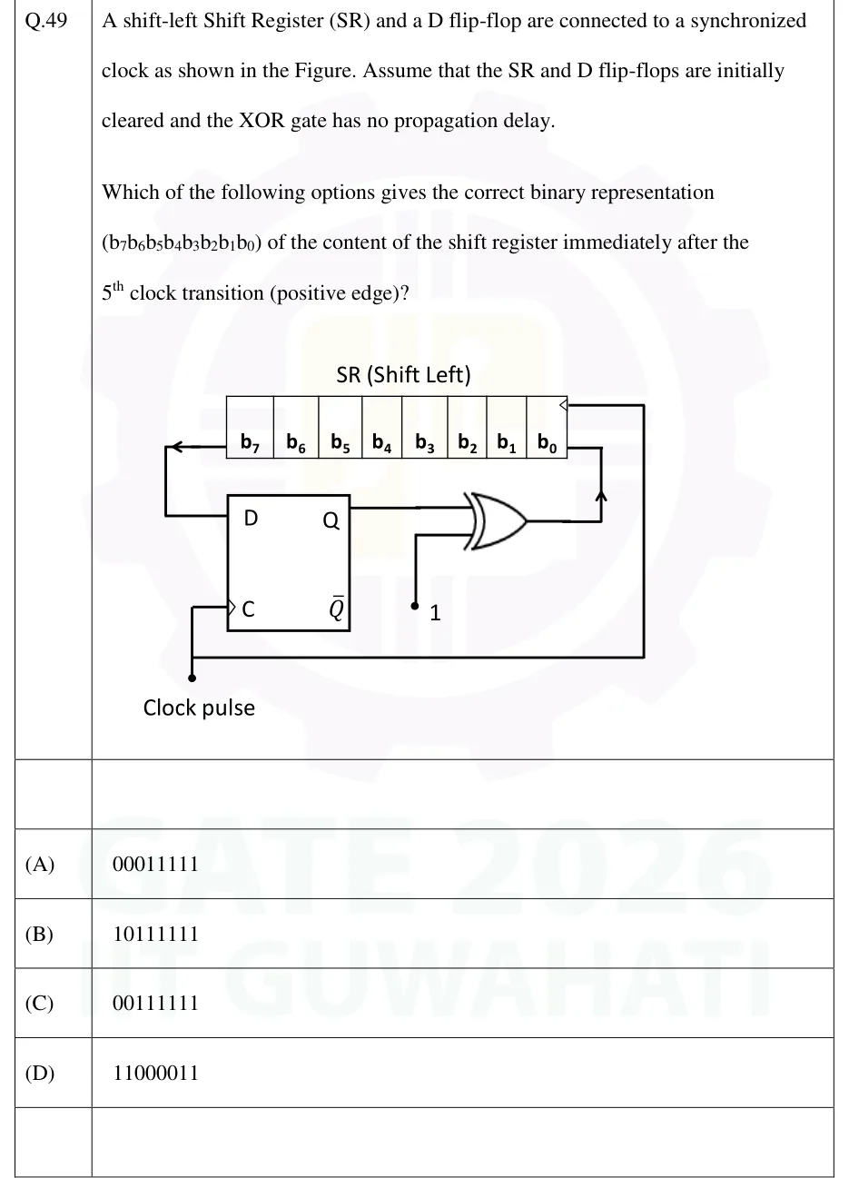
A shift-left Shift Register (SR) and a D flip-flop are connected to a synchronized clock as shown in the Figure. Assume that the SR and D flip-flops are initially cleared and the XOR gate has no propagation delay.
Which of the following options gives the correct binary representation of the content of the shift register immediately after the clock transition (positive edge)?
 Tap to open full size
An 8-bit shift register labelled 'SR (Shift Left)' with cells b7 b6 b5 b4 b3 b2 b1 b0 from left to right. Its clock input (a small triangle) is at the top-right corner next to b0. The serial output is taken from b7 (an arrow leaves b7 to the left) and is wired down to the D input of a D flip-flop. The flip-flop's Q output goes to one input of a 2-input XOR gate. The other XOR input is tied to constant logic 1. The XOR output is wired up into b0 (an arrow points up into b0), so it is the serial input of the shift-left register. The flip-flop's Q-bar output is unconnected. A single 'Clock pulse' line drives the flip-flop's clock input C (positive edge, no bubble). The same line runs along the bottom and up the right side to the shift register's clock input, so both are clocked together.
The initial state of in the digital circuit shown below is 1011.
The new value of after two rising edges of the clock (CLK) will be ______.
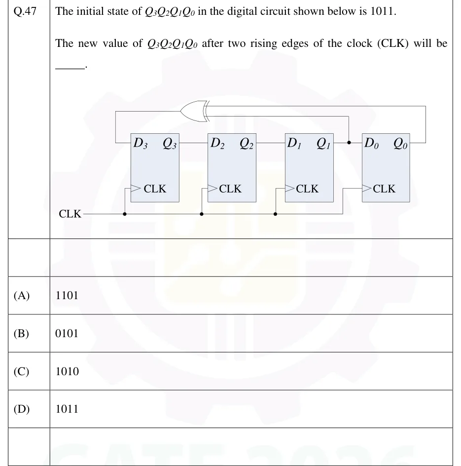 Tap to open full size
Four positive-edge-triggered D flip-flops drawn left to right: FF3 (D_3, Q_3), FF2 (D_2, Q_2), FF1 (D_1, Q_1), FF0 (D_0, Q_0). All four CLK inputs (plain triangle, no bubble) are tied to one common CLK line. Shift chain: Q_3 feeds D_2, Q_2 feeds D_1, Q_1 feeds D_0. A two-input XOR gate sits above the chain, drawn facing left. One XOR input is taken from a junction dot on the Q_1 to D_0 wire; the other XOR input is a feedback wire from Q_0, which runs up and back over the top of the circuit. The XOR output runs left and down into D_3. So D_3 = Q_1 XOR Q_0, D_2 = Q_3, D_1 = Q_2, D_0 = Q_1.
1101
0101
1010
1011
A positive-edge-triggered sequential circuit is shown below. There are no timing violations in the circuit. Input is set to logic '0' and is set to logic '1' at all times. The timing diagram of the inputs and are also shown below.
The sequence of output from time to is ________.
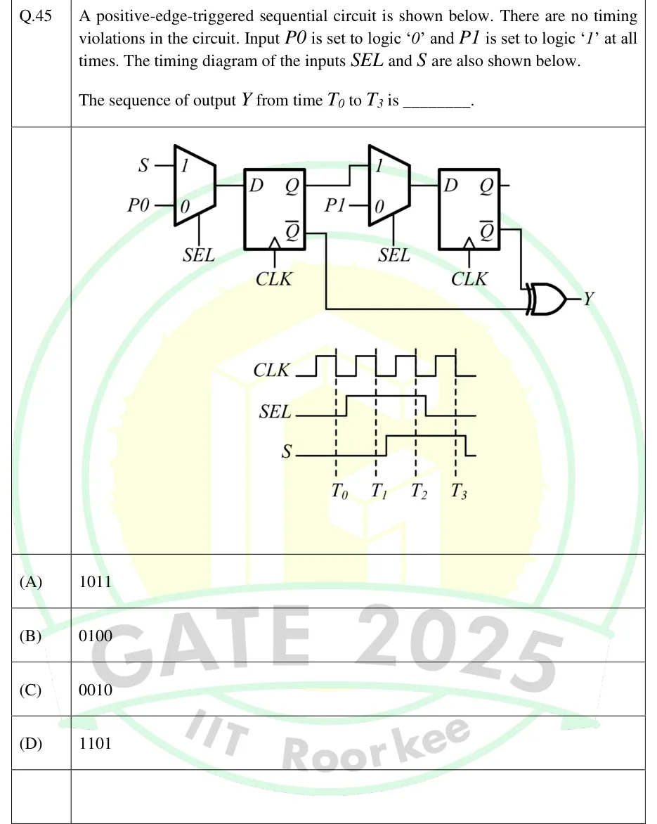 Tap to open full size
Circuit: a 2:1 MUX (MUX1) has input 1 = S, input 0 = P0 and select line SEL. Its output drives the D input of D flip-flop FF1, which is positive-edge triggered on CLK. The Q output of FF1 goes to input 1 of a second 2:1 MUX (MUX2). Input 0 of MUX2 is P1, and its select line is SEL. The MUX2 output drives the D input of D flip-flop FF2, also positive-edge triggered on CLK. FF2's Q output is an unconnected stub. A 2-input XOR gate has output Y. One XOR input is the Q-bar output of FF2. The other XOR input is the Q-bar output of FF1, routed down and along beneath the circuit. Timing diagram: CLK starts low and has four pulses. Vertical dashed lines labelled T0, T1, T2 and T3 fall on the four falling edges of CLK, so each rising edge lies between the previous dashed line and the next. SEL is 0 until just after T0 (before the next rising edge), then 1 until just after T2 (again before the next rising edge), then 0. S is 0 until just after T1 (before the next rising edge), then 1 until just after T3, then 0.
1011
0100
0010
1101
In the circuit shown below, the AND gate has a propagation delay of 1 ns. The edge-triggered flip-flops have a set-up time of 2 ns, a hold-time of 0 ns, and a clock-to-Q delay of 2 ns.
The maximum clock frequency (in MHz, rounded off to the nearest integer) such that there are no setup violations is ________.
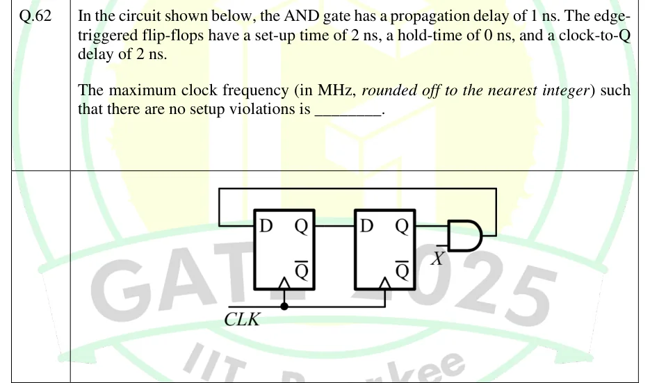 Tap to open full size
Two edge-triggered D flip-flops, FF1 (left) and FF2 (right), each drawn with outputs Q and Q and a clock input marked with the edge-trigger triangle. A common line CLK drives the clock inputs of both flip-flops. Q of FF1 is wired directly to D of FF2. Q of FF2 feeds one input of a 2-input AND gate; the other AND input is an external signal X. The AND gate output loops back along the top of the figure to D of FF1. The Q outputs of both flip-flops are unconnected.
The clock frequency of the digital circuit shown in the figure is 12 MHz. The frequencies of the output (F) corresponding to Control = 0 and Control = 1, respectively, are
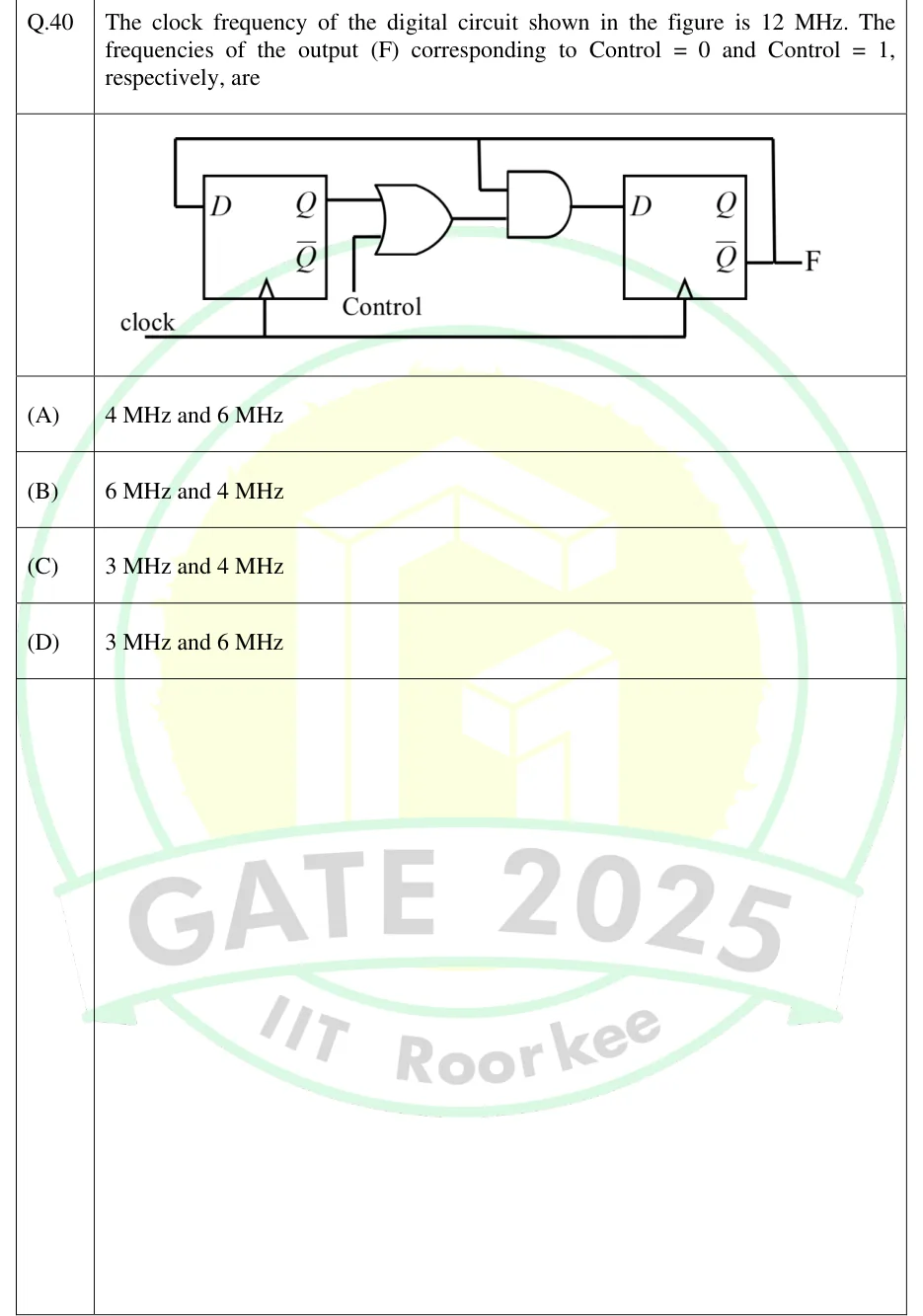 Tap to open full size
Two positive-edge-triggered D flip-flops, FF1 (left) and FF2 (right), share one clock line labelled 'clock' (edge-triggered clock inputs marked with a triangle on both). FF2's complemented output Q_2 is the circuit output F. A feedback wire from Q_2 (F) runs up across the top and back to the D input of FF1, so D_1 = Q_2; the same top wire has a branch that goes down into one input of a 2-input AND gate. A 2-input OR gate takes Q_1 (true output of FF1) and an external input labelled 'Control'. The OR output is the second input of the AND gate. The AND output drives the D input of FF2, so D_2 = Q_2 (Q_1 + Control). Q_1 is unconnected.
4 MHz and 6 MHz
6 MHz and 4 MHz
3 MHz and 4 MHz
3 MHz and 6 MHz
The sequence of states of the given synchronous sequential circuit is ________.
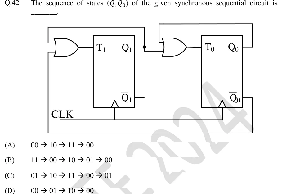 Tap to open full size
Two positive-edge-triggered T flip-flops share a common clock line CLK (the clock inputs are drawn with a triangle and no bubble). Flip-flop 1 (left) has input T_1 and outputs Q_1 and Q_1; Q_1 is not connected to anything. Flip-flop 0 (right) has input T_0 and outputs Q_0 and Q_0. OR gate 1 drives T_1. Its top input is fed back from Q_1: a wire leaves the junction dot on the Q_1 output, goes up, runs left and comes down into the gate. Its bottom input is Q_0: a wire leaves Q_0, goes right, down, left along the bottom of the drawing and up into the gate. So T_1 = Q_1 + Q_0. OR gate 2 drives T_0. One input is Q_1, taken straight from the junction dot. The other is Q_0, fed back through a wire that goes right from Q_0, up, left along the top and down into the gate. So T_0 = Q_1 + Q_0. There are no external inputs other than CLK.
00 → 10 → 11 → 00
11 → 00 → 10 → 01 → 00
01 → 10 → 11 → 00 → 01
00 → 01 → 10 → 00
In the circuit, the present value of is 1. Neglecting the delay in the combinatorial circuit, the values of and , respectively, after the application of the clock will be
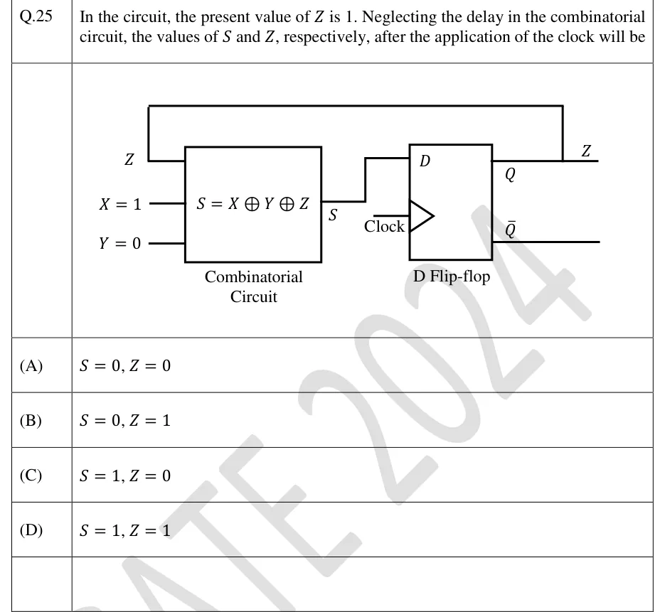 Tap to open full size
A combinatorial circuit block labelled S = X Y Z has three inputs: Z (top, fed back), X = 1 (middle) and Y = 0 (bottom). Its output S drives the D input of a D flip-flop, whose clock input is marked 'Clock' with an edge-trigger triangle. The flip-flop's Q output is labelled Z; a feedback wire runs from Q over the top of the diagram back to the Z input of the combinatorial circuit. The Q output is drawn but not connected to anything. Labels under the blocks: 'Combinatorial Circuit' and 'D Flip-flop'.
In the figure shown, the positive edge triggered D flip-flops are initially reset to Q = 0. The logic gates and the multiplexers have no propagation delay. After reset, a train of clock pulses (CLK) are applied. The logic-states of the inputs DIN, S and the clock pulses are also shown in the figure. Assuming no timing violations, the sequence of output Y from the 3rd clock to the 5th clock, is
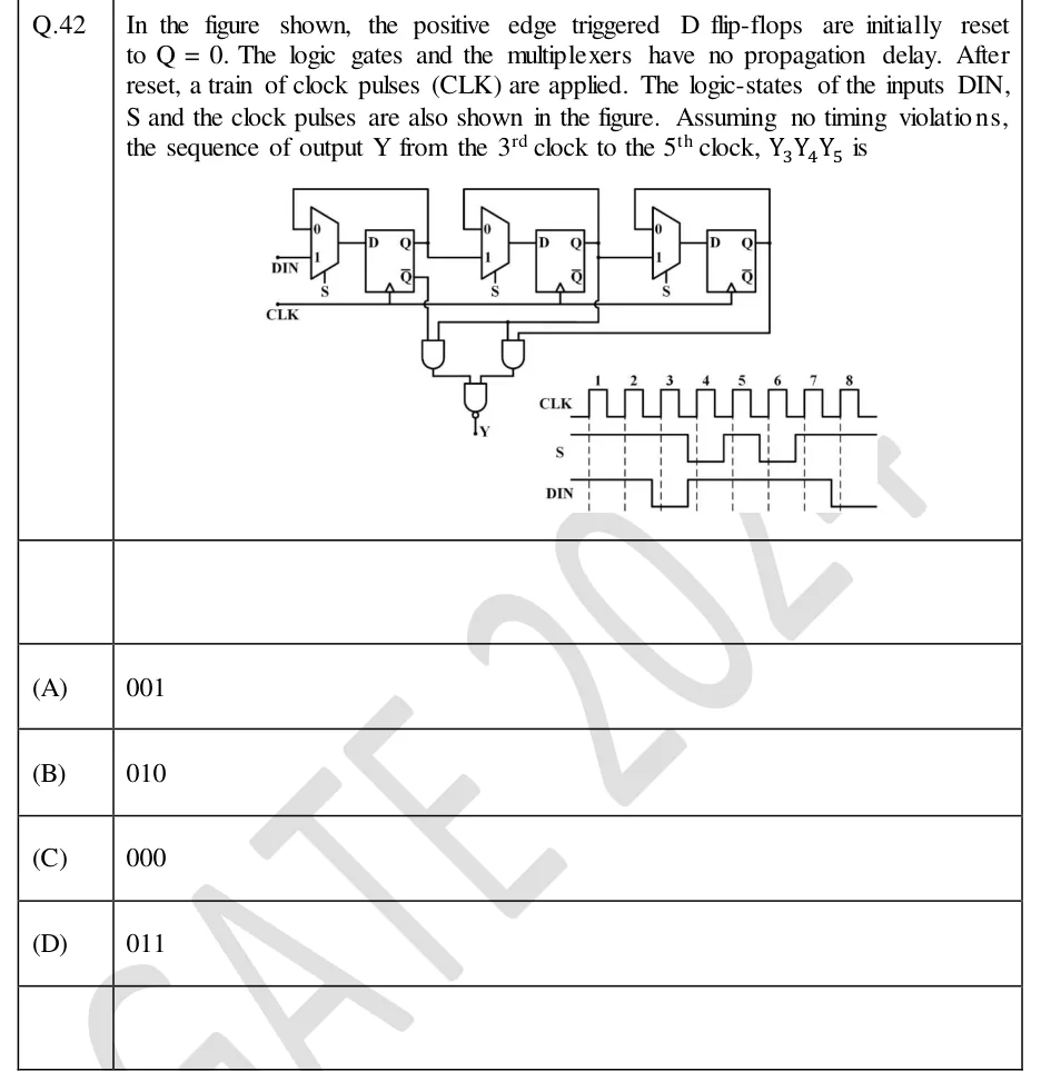 Tap to open full size
Circuit: three identical stages, each a 2:1 MUX (inputs labelled 0 on top and 1 below, select line S common to all three) whose output drives the D input of a positive-edge-triggered D flip-flop; all three clock inputs are tied to the common CLK line. Stage 1: MUX input 0 = Q1 (fed back from its own Q), MUX input 1 = DIN. Stage 2: MUX input 0 = Q2 (own feedback), MUX input 1 = Q1. Stage 3: MUX input 0 = Q3 (own feedback), MUX input 1 = Q2. So S = 1 shifts right (DIN -> Q1 -> Q2 -> Q3) and S = 0 holds. Output logic: left 2-input AND gate has inputs Q̄1 (complement output of FF1) and Q2; right 2-input AND gate has inputs Q2 and Q3; both AND outputs go to a 2-input NAND gate whose output is Y. Q̄2 and Q̄3 are unconnected. Timing diagram: CLK shows 8 pulses numbered 1 to 8, dashed vertical lines at each rising edge. S: high from the start through rising edge 3, goes low between edges 3 and 4, back high between edges 4 and 5, low between edges 5 and 6, high between edges 6 and 7 and stays high through edge 8 (S at edges 1-8 = 1,1,1,0,1,0,1,1). DIN: high through edge 2, goes low between edges 2 and 3, goes high between edges 3 and 4, stays high through edge 7, goes low between edges 7 and 8 (DIN at edges 1-8 = 1,1,0,1,1,1,1,0).
001
010
000
011
The synchronous sequential circuit shown below works at a clock frequency of 1 GHz. The throughput, in Mbits/s, and the latency, in ns, respectively, are
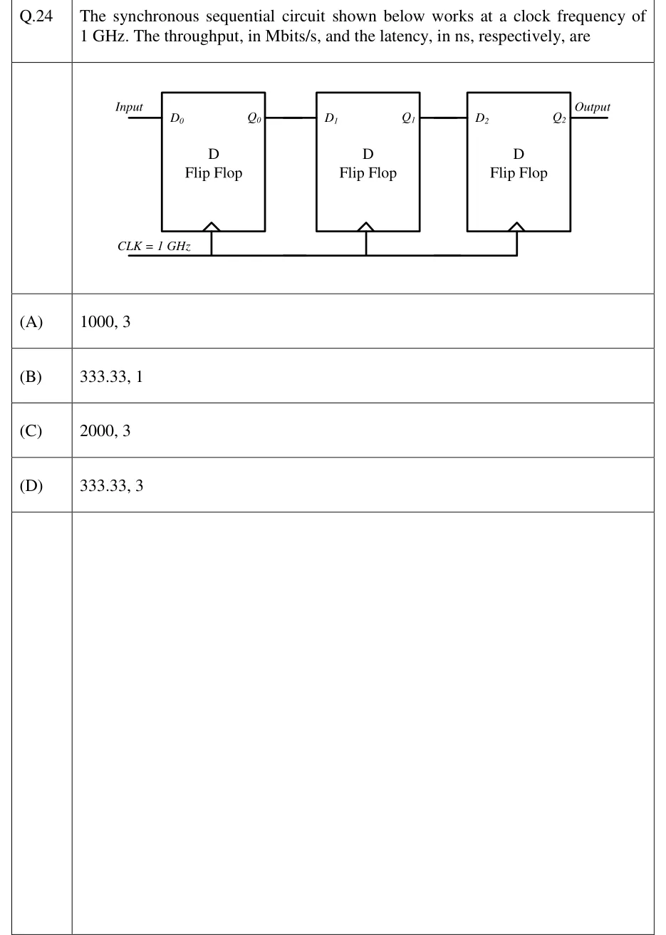 Tap to open full size
Three positive-edge-triggered D flip-flops connected in cascade (a 3-stage serial-in serial-out shift register). 'Input' drives D_0 of the first flip-flop; its output Q_0 drives D_1 of the second flip-flop; Q_1 drives D_2 of the third flip-flop; Q_2 is the 'Output'. Each box is labelled 'D Flip Flop' and has a clock triangle at the bottom. All three clock inputs are tied to a common line labelled CLK = 1 GHz.
1000, 3
333.33, 1
2000, 3
333.33, 3
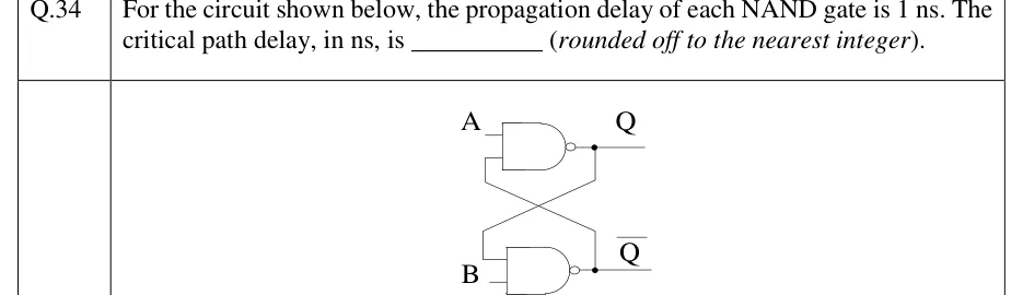
For the circuit shown below, the propagation delay of each NAND gate is 1 ns. The critical path delay, in ns, is ________ (rounded off to the nearest integer).
 Tap to open full size
Two cross-coupled 2-input NAND gates (a NAND SR latch). Top NAND gate: upper input is external input A; lower input is fed back from the output of the bottom NAND gate. Its output is labelled Q (a dot marks the junction where Q is tapped for feedback). Bottom NAND gate: upper input is fed back from the Q output of the top gate; lower input is external input B. Its output is labelled Q (with a junction dot where it is tapped for feedback). The two feedback wires cross each other in an X between the gates. No clock is present.
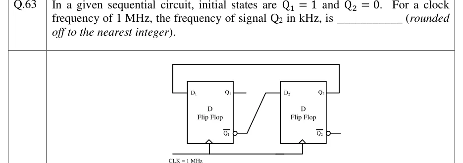
In a given sequential circuit, initial states are and . For a clock frequency of , the frequency of signal in kHz, is ________ (rounded off to the nearest integer).
 Tap to open full size
Two positive-edge-triggered D flip-flops (clock input shown as a plain triangle with no bubble) share one clock, labelled CLK = 1 MHz. Flip-flop 1 has input D_1 and outputs Q_1 and Q_1. Flip-flop 2 has input D_2 and outputs Q_2 and Q_2. A feedback wire runs from the Q_2 output, up over the top of both flip-flops, and down into D_1, so D_1 = Q_2. A diagonal wire joins the Q_1 output (with its bubble) to D_2, so D_2 = Q_1. The Q_1 output and the Q_2 output are short stubs that connect to nothing else. This is a 2-bit twisted-ring (Johnson) counter.
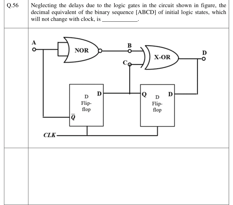
Neglecting the delays due to the logic gates in the circuit shown in figure, the decimal equivalent of the binary sequence [ABCD] of initial logic states, which will not change with clock, is ________.
 Tap to open full size
Two D flip-flops, FF1 (left) and FF2 (right), both driven by a common CLK line. FF1 has its D input pin drawn on its right side and its Q output on its lower-left side. FF2 has its Q output on its left side and its D input on its right side. Node A (top-left terminal) is tied by a wire running down to FF1's Q output, so A = Q_1. A drives both inputs of a two-input NOR gate (both inputs shorted together, so the NOR acts as an inverter); the NOR output is node B. B and node C are the two inputs of a two-input X-OR gate whose output is node D (top-right terminal). Node D is wired down to the D input of FF2. FF2's Q output is wired left to the D input of FF1, and a junction on that wire goes up to node C, so C = Q_2 = D_1. So: A = Q_1, B = A (NOR of A with A), C = Q_2, D = B C, D_1 = Q_2, D_2 = D.
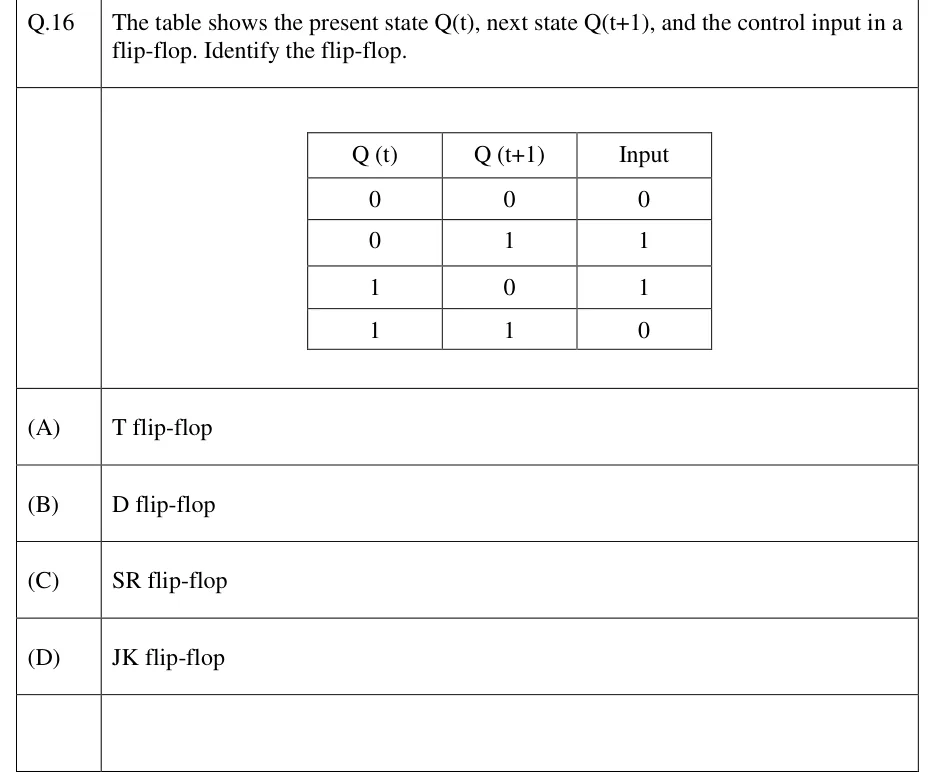
The table shows the present state Q(t), next state Q(t+1), and the control input in a flip-flop. Identify the flip-flop.
| Q (t) | Q (t+1) | Input |
|---|---|---|
| 0 | 0 | 0 |
| 0 | 1 | 1 |
| 1 | 0 | 1 |
| 1 | 1 | 0 |
 Tap to open full size
A table with three columns headed Q (t), Q (t+1) and Input, and four rows: (Q(t), Q(t+1), Input) = (0, 0, 0), (0, 1, 1), (1, 0, 1), (1, 1, 0).
T flip-flop
D flip-flop
SR flip-flop
JK flip-flop
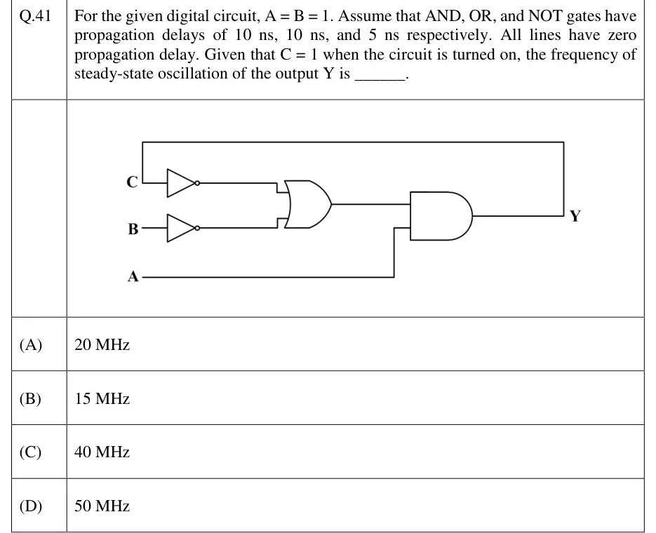
For the given digital circuit, A = B = 1. Assume that AND, OR, and NOT gates have propagation delays of 10 ns, 10 ns, and 5 ns respectively. All lines have zero propagation delay. Given that C = 1 when the circuit is turned on, the frequency of steady-state oscillation of the output Y is ______.
 Tap to open full size
Combinational loop. Input C goes through a NOT gate to the first input of a 2-input OR gate. Input B goes through a second NOT gate to the second input of the same OR gate. The OR output goes to the first input of a 2-input AND gate; input A goes directly to the second input of the AND gate. The AND output is the output Y, and a wire runs from Y back up and around to the left to become input C (Y is fed back to C).
20 MHz
15 MHz
40 MHz
50 MHz
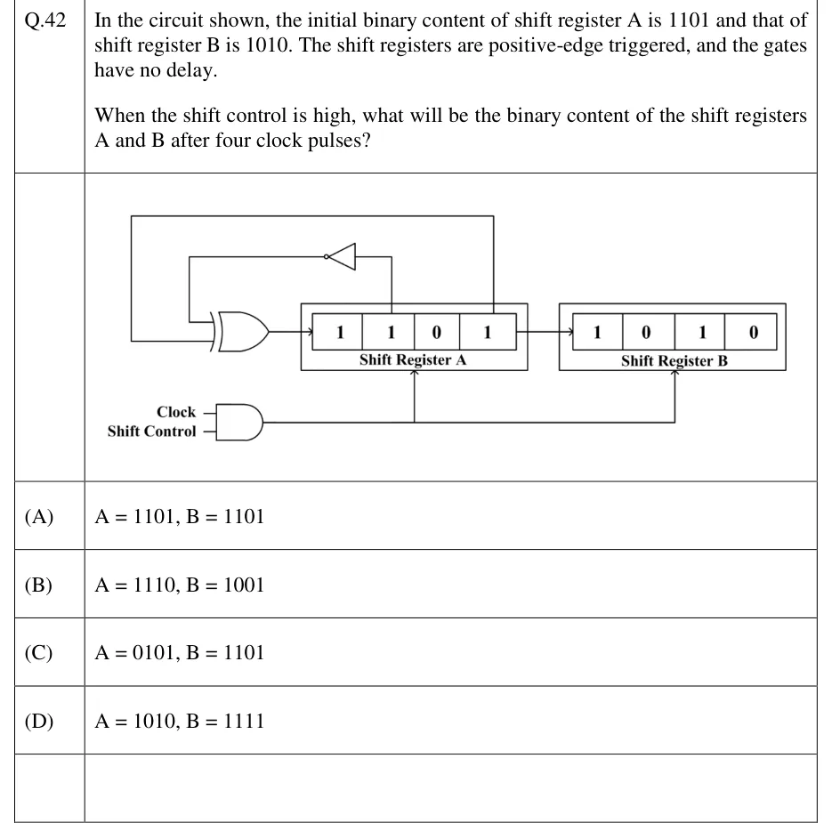
In the circuit shown, the initial binary content of shift register A is 1101 and that of shift register B is 1010. The shift registers are positive-edge triggered, and the gates have no delay.
When the shift control is high, what will be the binary content of the shift registers A and B after four clock pulses?
 Tap to open full size
Two 4-bit shift registers in cascade, both shifting to the right. Shift Register A holds, left to right, 1 1 0 1 (call the cells A1 A2 A3 A4). Shift Register B holds, left to right, 1 0 1 0 (B1 B2 B3 B4). The serial output of A (the rightmost cell A4) feeds the serial input of B (its leftmost cell). The serial input of A (leftmost cell A1) comes from a 2-input XOR gate. XOR input 1: a wire from the top of the second cell of A (A2) goes up and into a NOT gate (triangle pointing left with the bubble on its left-hand output); the inverter output runs left and down into the upper XOR input, so that input is A2 complemented. XOR input 2: a wire from the top of the rightmost cell of A (A4) goes up, runs left across the top of the figure, down the left side and right into the lower XOR input. Clocking: a 2-input AND gate takes 'Clock' and 'Shift Control'; its output is the common clock of both registers (drawn as arrows into the bottom of Shift Register A and Shift Register B). The registers are positive-edge triggered.
A = 1101, B = 1101
A = 1110, B = 1001
A = 0101, B = 1101
A = 1010, B = 1111
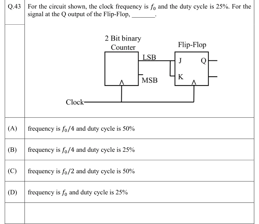
For the circuit shown, the clock frequency is and the duty cycle is 25%. For the signal at the Q output of the Flip-Flop, ________.
 Tap to open full size
A block labelled '2 Bit binary Counter' has two outputs on its right side: LSB (upper) and MSB (lower). The MSB output is a short stub that connects to nothing. The LSB output runs to the J input of a block labelled 'Flip-Flop' (a JK flip-flop). A short vertical wire joins the J line to the K input, so J and K are tied together and both get the counter's LSB. The flip-flop has an output labelled Q on the right and a second, unlabelled output stub below it. The counter and the flip-flop each have a clock input drawn as a triangle with no bubble, so both trigger on the rising edge. One line labelled 'Clock' drives both clock inputs.
frequency is and duty cycle is 50%
frequency is and duty cycle is 25%
frequency is and duty cycle is 50%
frequency is and duty cycle is 25%
A MOD 2 and a MOD 5 up-counter when cascaded together results in a MOD ______ counter. (in integer)
The maximum clock frequency in MHz of a 4-stage ripple counter, utilizing flip-flops, with each flip-flop having a propagation delay of 20 ns, is ________. (round off to one decimal place)
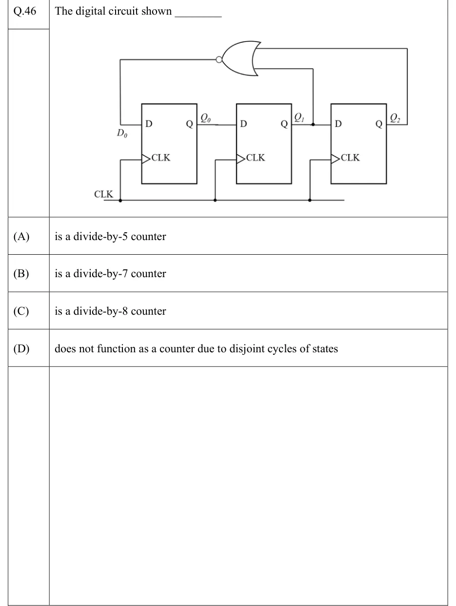
The digital circuit shown ________
 Tap to open full size
Three positive-edge-triggered D flip-flops (clock inputs drawn with a triangle, no bubble) share one common clock line CLK. Left to right: FF0 has input D (labelled D_0) and output Q_0; FF1 has D = Q_0 and output Q_1; FF2 has D = Q_1 and output Q_2. So the three flip-flops form a serial shift register Q_0 -> Q_1 -> Q_2. A two-input NOR gate (OR symbol with an output bubble) takes Q_1 (tapped at a junction dot between FF1 and FF2) and Q_2 (fed back from the rightmost output) as inputs; its output is wired back to D_0, the D input of the first flip-flop. There are no other inputs, no preset or clear.
is a divide-by-5 counter
is a divide-by-7 counter
is a divide-by-8 counter
does not function as a counter due to disjoint cycles of states
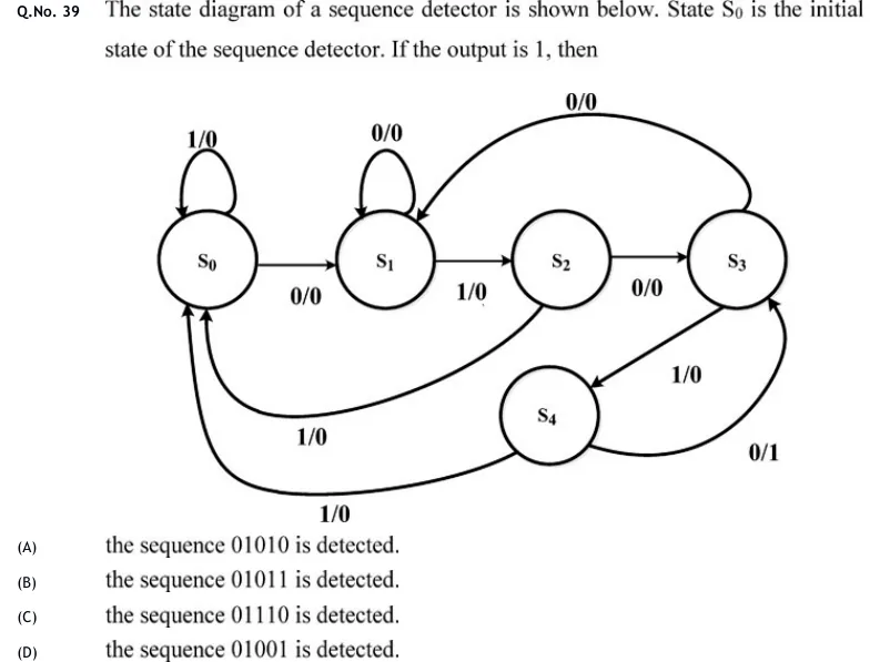
The state diagram of a sequence detector is shown below. State is the initial state of the sequence detector. If the output is 1, then
 Tap to open full size
Mealy state diagram with five states S0, S1, S2, S3, S4. S0, S1, S2 and S3 sit in a row from left to right, and S4 sits below, between S2 and S3. Each edge is labelled input/output. Edges: S0 has a self-loop labelled 1/0; S0 -> S1 labelled 0/0; S1 has a self-loop labelled 0/0; S1 -> S2 labelled 1/0; S2 -> S3 labelled 0/0; S2 -> S0 labelled 1/0 (a curve running under the row back to S0); S3 -> S1 labelled 0/0 (a curve running over the top from S3 back to S1); S3 -> S4 labelled 1/0; S4 -> S3 labelled 0/1 (a curve from the lower-right side of S4 up to the lower-right of S3); S4 -> S0 labelled 1/0 (a long curve along the bottom back to S0).
the sequence 01010 is detected.
the sequence 01011 is detected.
the sequence 01110 is detected.
the sequence 01001 is detected.
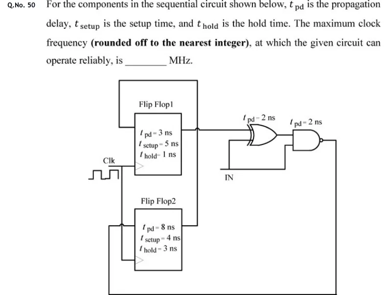
For the components in the sequential circuit shown below, is the propagation delay, is the setup time, and is the hold time. The maximum clock frequency (rounded off to the nearest integer), at which the given circuit can operate reliably, is ________ MHz.
 Tap to open full size
Two positive-edge-triggered flip-flops share one clock (Clk, drawn as a square wave on the left, wired to the clock input (triangle) of both). Flip Flop1 is labelled t_pd = 3 ns, t_setup = 5 ns, t_hold = 1 ns. Flip Flop2 is labelled t_pd = 8 ns, t_setup = 4 ns, t_hold = 3 ns. Flip Flop1's output (right side) runs right to one input of a 2-input XOR gate (t_pd = 2 ns). The XOR's second input comes from an external line marked IN, and IN also feeds the second input of a 2-input NAND gate (t_pd = 2 ns). The XOR output goes to the NAND's first input. The NAND output runs right, down along the bottom of the drawing, back left and up into the D input (left side) of Flip Flop2. Flip Flop2's output (right side) runs right to a vertical wire. That wire goes up, crosses Flip Flop1's output line at a hop (no connection), continues over the top of Flip Flop1 and comes down into Flip Flop1's D input (left side). So the two register-to-register paths are FF1 -> XOR -> NAND -> FF2 and FF2 -> FF1 directly.
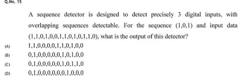
A sequence detector is designed to detect precisely 3 digital inputs, with overlapping sequences detectable. For the sequence (1,0,1) and input data (1,1,0,1,0,0,1,1,0,1,0,1,1,0), what is the output of this detector?
1,1,0,0,0,0,1,1,0,1,0,0
0,1,0,0,0,0,0,1,0,1,0,0
0,1,0,0,0,0,0,1,0,1,1,0
0,1,0,0,0,0,0,0,1,0,0,0
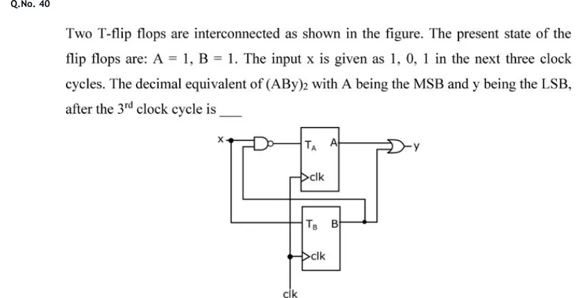
Two T-flip flops are interconnected as shown in the figure. The present state of the flip flops are: A = 1, B = 1. The input x is given as 1, 0, 1 in the next three clock cycles. The decimal equivalent of with A being the MSB and y being the LSB, after the 3rd clock cycle is ____
 Tap to open full size
Two T flip-flops, A (top) and B (bottom), share a common clock line labelled clk. Both clock inputs are edge-triggered (triangle, no bubble). Input x feeds one input of a 2-input NAND gate and, through a junction, also goes straight down and across to the T input of flip-flop B (so T_B = x). The second input of the NAND gate comes from output B: a wire leaves the NAND's lower input, runs down, crosses the clock line with no junction, and joins B's output at a junction dot. The NAND output drives T_A (so T_A = (x B)'). Output A and output B are the two inputs of an OR gate whose output is y (y = A + B). No other connections; the flip-flops have only T, clk and a single output (A or B).
A traffic signal cycles from GREEN to YELLOW, YELLOW to RED and RED to GREEN. In each cycle, GREEN is turned on for 70 seconds, YELLOW is turned on for 5 seconds and the RED is turned on for 75 seconds. This traffic light has to be implemented using a finite state machine (FSM). The only input to this FSM is a clock of 5 second period. The minimum number of flip-flops required to implement this FSM is ________.
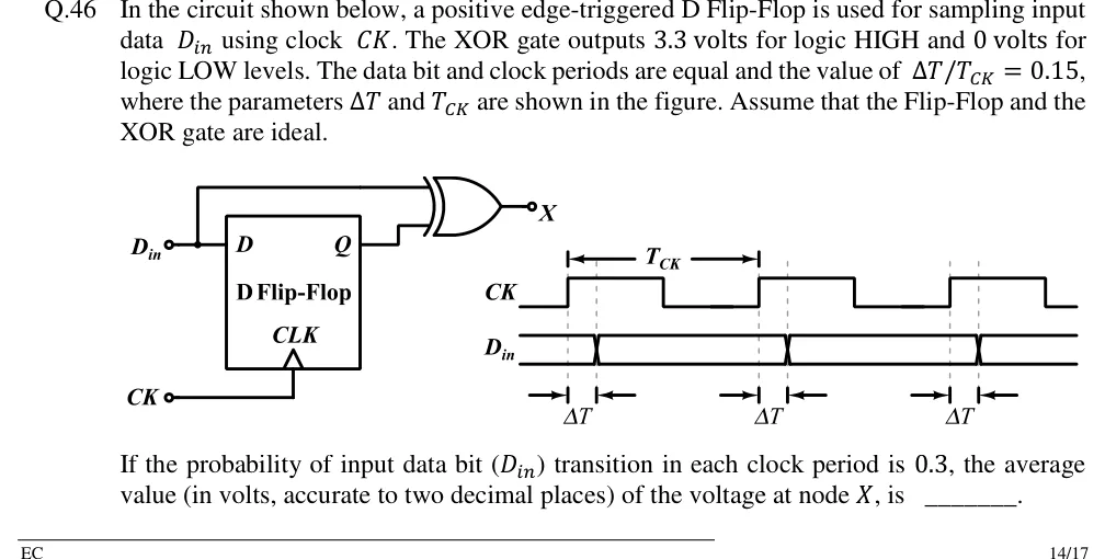
In the circuit shown below, a positive edge-triggered D Flip-Flop is used for sampling input data using clock . The XOR gate outputs 3.3 volts for logic HIGH and 0 volts for logic LOW levels. The data bit and clock periods are equal and the value of , where the parameters and are shown in the figure. Assume that the Flip-Flop and the XOR gate are ideal.
If the probability of input data bit () transition in each clock period is 0.3, the average value (in volts, accurate to two decimal places) of the voltage at node , is ______.
 Tap to open full size
Circuit (left): input terminal D_in feeds the D input of a D Flip-Flop; the same D_in node also branches up and over to the first (upper) input of a 2-input XOR gate. The flip-flop output Q goes to the second (lower) input of the XOR gate. The XOR output is node X. Input terminal CK drives the flip-flop's CLK input (edge-triggered, marked with a triangle). Timing diagram (right): CK is a square wave with period T_CK (marked between two successive rising edges), about 50% duty cycle; three rising edges are shown. D_in is drawn as a data-eye waveform (two parallel lines with crossovers) whose transitions (crossovers) occur a delay Δ T AFTER each rising edge of CK; the Δ T interval is marked between each rising edge (dashed line) and the following D_in crossover (dashed line), three times. The data bit period equals T_CK.
Which one of the following statements is true about the digital circuit shown in the figure
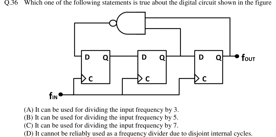 Tap to open full size
Three D flip-flops sit side by side. The figure does not name them; this solution calls them FF1, FF2 and FF3 from left to right. Each has a D input, a clock input C and one output Q. The clocks are edge-triggered (triangle symbol, no inversion bubble), so they trigger on the positive edge. All three clock inputs C are tied to one input, f_IN. Q of FF1 drives D of FF2, Q of FF2 drives D of FF3, and Q of FF3 is the circuit output f_OUT. A 2-input NAND gate sits above the flip-flops, drawn facing left with its bubble on the output. One input comes from Q3 (the f_OUT line) and the other from Q2 (the line from Q2 to D3). The NAND output goes back to D of FF1. So D1 = NAND(Q2, Q3), D2 = Q1 and D3 = Q2.
It can be used for dividing the input frequency by 3.
It can be used for dividing the input frequency by 5.
It can be used for dividing the input frequency by 7.
It cannot be reliably used as a frequency divider due to disjoint internal cycles.
For the 3-bit binary counter shown in the figure, the output increments at every positive transition in the clock (CLK). Assume ideal diodes and the starting state of the counter as 000. If output high is 1 V and output low is 0 V, the current (in mA) flowing through the 50 resistor during the 5 clock cycle is (up to one decimal place) ______.
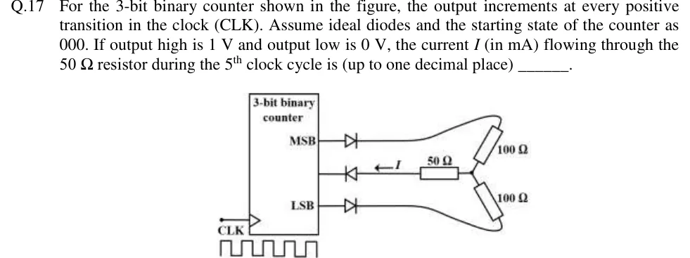 Tap to open full size
A block labelled '3-bit binary counter' has a clock input CLK on its lower left, marked with the edge-trigger triangle. A square-wave pulse train is drawn under CLK. The block has three outputs on its right side, from top to bottom: MSB, then the middle bit (unlabelled, just below MSB), then LSB (lower down). (1) MSB goes into a diode pointing away from the counter (anode at the MSB output, cathode on the right). From the cathode a wire curves up to a 100 Ω resistor, which runs down to a common junction node. (2) LSB goes into a diode pointing away from the counter (anode at the LSB output), and from its cathode a wire curves down to a second 100 Ω resistor, which runs up to the same junction node. (3) The junction node connects through a horizontal 50 Ω resistor to a diode pointing TOWARD the counter (anode on the resistor side, cathode at the middle-bit output). The current I is drawn with a left-pointing arrow in this branch, i.e. from the junction through the 50 Ω resistor and diode into the counter's middle-bit output.
A 2-bit synchronous counter using two - flip flops is shown. The expressions for the inputs to the - flip flops are also shown in the figure. The output sequence of the counter starting from is
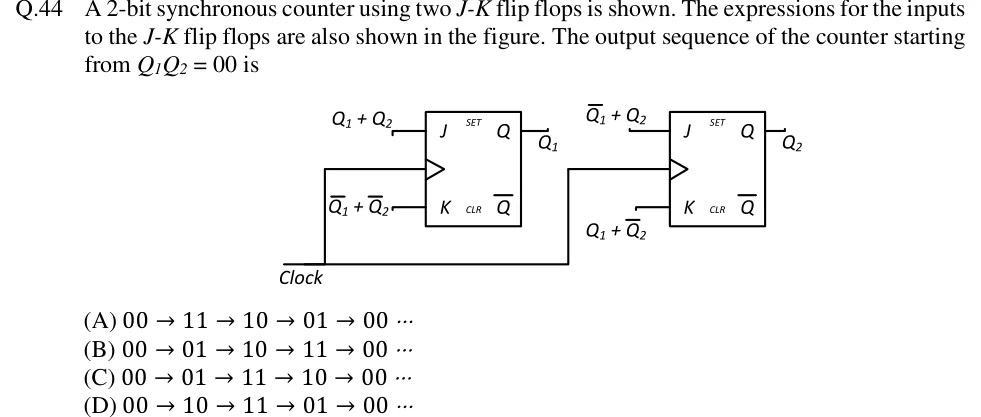 Tap to open full size
Two J-K flip-flops (each box labelled J, K, Q, Q-bar, SET, CLR) share one Clock line, so the counter is synchronous. The clock-input triangle carries no bubble (positive-edge triggered as drawn). Left flip-flop: output Q is labelled Q_1; its J input is labelled Q_1 + Q_2 and its K input is labelled Q_1 + Q_2. Right flip-flop: output Q is labelled Q_2; its J input is labelled Q_1 + Q_2 and its K input is labelled Q_1 + Q_2. SET and CLR are left unconnected. (Overbar = complement.)
PRACTICE
A 4-bit asynchronous (ripple) up counter is built from flip-flops whose clock-to-Q propagation delay is 12 ns each. Ignoring any decoding delay, the maximum clock frequency, in MHz, at which the counter always settles to the correct count before the next clock edge is ______ (round to two decimal places).
Answer: (accepted range )
In a ripple counter each flip-flop is clocked by the one before it. In the worst case (for example ) the change passes through all 4 stages.
Worst-case settling time ns.
MHz.
A positive-edge-triggered D flip-flop is to be made to behave exactly like a JK flip-flop by placing combinational logic in front of its D input. With the present output and an overline denoting the complement, the required input is
Answer: (A)
A D flip-flop's next state equals D, so D must equal the JK flip-flop's next state.
The JK characteristic equation is , hence .
Option C is the input that turns a T flip-flop, not a D flip-flop, into a JK. Option D gives for , which is wrong whenever .
Which of the following statements are correct?
A 4-bit Johnson (twisted-ring) counter cycles through 8 distinct states.
A 4-bit ring counter preset to 1000 leaves 12 of the 16 possible states unused.
The minimum number of states in a Moore machine that detects the pattern 1101, with overlapping allowed, is 4.
In a Mealy machine, the output can change between two clock edges if the input changes.
Answer: (A), (B), (D)
A: a Johnson counter with n flip-flops has 2n states, and . True.
B: a ring counter with n flip-flops uses n states, so states are unused. True.
C: a Moore detector for a pattern of length needs states: 0, 1, 2 or 3 bits matched, plus a detecting state whose output is 1. No two of these are equivalent, so the minimum is 5, not 4. False.
D: a Mealy output is a combinational function of the present input, so it changes as soon as the input changes, even between clock edges. True.
In a synchronous circuit, positive-edge-triggered flip-flop FF1 drives flip-flop FF2 through combinational logic. Both flip-flops have a clock-to-Q delay of 2 ns (minimum) to 3 ns (maximum), a setup time of 2 ns and a hold time of 1 ns. The logic has a longest-path delay of 9 ns and a shortest-path delay of 4 ns. The clock edge reaches FF2 1 ns earlier than it reaches FF1. Consider only the path from FF1 to FF2. The maximum clock frequency, in MHz, is ______ (round to two decimal places).
Answer: (accepted range )
Skew: ns, because the capturing flip-flop is clocked earlier.
Setup: ns.
Hold: ns ns. Hold is met, so setup alone limits the frequency.
MHz.
Three positive-edge-triggered D flip-flops form a synchronous circuit with state (MSB first), where , and . The circuit starts in 000. Which statement is correct?
It is a mod-6 counter and is not self-starting.
It is a mod-5 counter, and every unused state enters the counting cycle (self-starting).
It is a mod-5 counter, but the unused states 010 and 101 form a separate closed loop (lock-out).
It is a mod-8 counter.
Answer: (B)
From 000: , , , so the next state is 001. From 001 the next state is 011. From 011: , giving 110. From 110 the next state is 100, and from 100 it is 000.
The cycle has 5 states, so the circuit is a mod-5 counter.
Unused states: ; ; . All of them reach the cycle, so the counter is self-starting.
Answer B. For comparison, a 3-bit Johnson counter () is mod-6 with the lock-out loop . The NOR feedback here removes one state and also breaks that loop.
OFFICIAL GATE 2027 SYLLABUS WORDING
Copied from the GATE 2027 syllabus; see all 2027 syllabi.
GATE EC
Sequential Circuits: Latches and flip-flops, counters, shift-registers, finite state machines, propagation delay, setup and hold time, critical path delay
GATE EE
sequential logic circuits
GATE IN
sequential circuits, finite state machines, flipflops, shift registers, timers and counters
Preparing in Kolkata? IAE Academy's course for GATE ECE, GATE EE or GATE IN.