IAE Academy

IN THE EC AND IN SYLLABUS

Logic families and CMOS logic gates

Logic families are compared on a few datasheet parameters: the voltage thresholds , , , , the noise margins, fan-out, propagation delay, power and the power-delay product. The standard calculations on this topic find one of these parameters, or a CMOS inverter's switching threshold, noise margins or dynamic power. Every static complementary CMOS gate is an NMOS pull-down network together with a PMOS pull-up network that is its dual. Reading or designing such a network, and counting its transistors, uses one rule: in the pull-down network series means AND and parallel means OR, and the output is the complement.

7 previous-year questions · 7 solved · 6 practice questions

Conventions and logic-family parameters

Conventions used in these notes. We use positive logic, so the HIGH voltage level is logic 1. The complement of is written with an overline, . All voltage parameters are the worst-case datasheet limits:

  • is the minimum guaranteed HIGH output voltage.
  • is the maximum guaranteed LOW output voltage.
  • is the minimum input voltage guaranteed to be read as 1.
  • is the maximum input voltage guaranteed to be read as 0.

An input between and is in the undefined region.

Currents are used as magnitudes:

  • is the largest current an output can source while HIGH.
  • is the largest current an output can sink while LOW.
  • is the current one input draws when HIGH.
  • is the current that flows out of one input when LOW.

Datasheets give a current flowing out of a pin a negative sign (for example mA). Drop the sign when you calculate fan-out.

A logic family works only if every worst-case output is a valid input for the next gate: and . The gaps between these levels are the noise margins. A noise margin is the largest noise voltage that can be added to a worst-case output before the driven input can misread it.

Fan-out is the maximum number of inputs of the same family that one output can drive while still meeting its guaranteed output levels. Fan-in is the number of inputs a gate has. Propagation delay measures speed and power dissipation measures the power a gate draws. Their product, the power-delay product, is a single figure of merit.

HIGH-LEVEL NOISE MARGIN

Uses worst-case values: the minimum and the minimum .

LOW-LEVEL NOISE MARGIN

Uses worst-case values: the maximum and the maximum . The family's noise margin is the smaller of and .

DC FAN-OUT

All currents are magnitudes. Round each ratio down, then take the smaller. A CMOS input draws almost no DC current, so CMOS fan-out is limited by load capacitance (it slows the gate), not by this formula.

PROPAGATION DELAY

is the time from the 50% point of the input edge to the 50% point of the output's HIGH-to-LOW edge. is the same for the output's LOW-to-HIGH edge. Rise and fall times are measured from 10% to 90%. If a question asks for the worst-case delay, use instead.

AVERAGE STATIC POWER OF A GATE

Assumes the output spends equal time HIGH and LOW (50% duty cycle). and are the supply currents of one gate with its output HIGH and LOW. If a datasheet gives them for a whole package, divide by the number of gates in the package.

POWER-DELAY PRODUCT

The energy per switching event. It is a figure of merit, and lower is better. Units: mW times ns gives pJ.

WORKED EXAMPLE

A logic family has these worst-case limits: V, V, V, V. The currents are mA, mA, A and mA. The delays are ns and ns. With V the supply current is mA with the output HIGH and mA with it LOW. Find the noise margins, fan-out, , average power and power-delay product.

Solution
  1. V and V. The family's noise margin is the smaller one, 0.4 V.

  2. LOW state: . HIGH state: . Fan-out .

  3. ns.

  4. mW.

  5. pJ.

Answer: V and V. Fan-out = 12, ns, mW and PDP = 110 pJ.

EXAM TIP

For fan-out, work out both the LOW-state and HIGH-state ratios, round each one down and keep the smaller. A ratio of 12.8 means 12 loads, never 13. The noise margin of a family is likewise the smaller of and .

TTL and ECL families (IN)

TTL (transistor-transistor logic) is a bipolar family that runs from a single +5 V supply. Its basic gate is the NAND: a multi-emitter input transistor performs the AND and the stages after it invert. In standard TTL the transistors are driven into saturation. Removing the stored base charge takes time (the storage time), and this is a large part of standard TTL's delay. Schottky variants (74S, 74LS) clamp the base-collector junction of every transistor that would otherwise saturate with a Schottky diode. This keeps those transistors out of deep saturation and cuts the storage delay.

An unconnected (floating) TTL input behaves as logic 1, because no current can flow out of that emitter. In practice, tie unused inputs to a defined level anyway.

Standard 74-series TTL datasheet limits:

  • Voltages: V, V, V and V, which give V.
  • Currents: mA, mA, mA and A. Both current ratios equal 10, so the fan-out is 10.

TTL output stage

How it works

Consequence

Totem-pole (active pull-up)

An upper transistor pulls the output HIGH and a lower transistor pulls it LOW. In steady state only one of them is on.

Output impedance is low in both states, so load capacitance charges quickly. Two totem-pole outputs must never be tied together: if one is HIGH and the other LOW, a large current flows through both. A short current spike occurs at each switching edge while both transistors conduct.

Open-collector

Only the lower (pull-down) transistor is present. An external pull-up resistor to is required.

Outputs can be tied together as a wired-AND: the line is HIGH only when every output is off. The output can also sink current from an external load, such as an LED with a series resistor, within its rating. The rising edge is slower because it is set by the pull-up resistor and the load capacitance.

Tri-state

An enable input turns both output transistors off, which leaves the output in a high-impedance state Z.

Several outputs can share one bus line, as long as only one of them is enabled at a time.

PULL-UP RESISTOR RANGE FOR OPEN-COLLECTOR OUTPUTS

Here open-collector outputs are wired together and drive load inputs. : a single output that is LOW must sink the resistor current plus without exceeding . : with every output off, the leakage current plus flowing through must not pull the line below . Choose with .

ECL (emitter-coupled logic) is built around a differential pair of emitter-coupled transistors. The pair steers a nearly constant current to one side or the other according to whether the input is above or below a reference voltage . The transistors switch between cut-off and the active region and never saturate, so there is no storage-time delay. This, together with its small logic swing, is why ECL is the fastest of the classical logic families.

Other ECL features:

  • Emitter-follower outputs give low output impedance and a high fan-out.
  • The basic ECL gate provides both an OR and a NOR output.
  • is grounded and is negative (typically V), which makes the output less sensitive to noise on the supply.
  • The logic swing is small (under 1 V), so the noise margins are small.
  • The supply current is almost the same whether the output is HIGH or LOW. ECL therefore has the highest static power of the three families, but produces only small supply-current spikes when it switches.
  • Emitter-follower outputs can be tied together as a wired-OR.

Property

TTL

ECL

Static CMOS

Devices and operating mode

BJTs, driven into saturation (standard TTL)

BJTs, never saturated (cut-off or active)

Complementary MOSFETs used as switches

Basic gate

NAND

OR/NOR (both outputs available)

NAND, NOR or any single-stage inverting function

Supply

+5 V

, negative (typically V)

A single over a wide range

Speed

Moderate

Fastest

Depends on and load capacitance

Power

Moderate, mostly static

Highest, nearly constant

Static power close to 0; dynamic power rises with frequency

Noise margin

0.4 V (standard series)

Small (logic swing under 1 V)

Large, a sizeable fraction of

Fan-out

10 (standard series)

High

Very large at DC, but limited by capacitive loading

Wired logic

Wired-AND, with open-collector outputs only

Wired-OR of emitter-follower outputs

Wired-AND with open-drain outputs only; never with ordinary push-pull outputs

EXAM TIP

A floating TTL input reads as 1. A floating CMOS input has no defined level and can leave both transistors of its input stage partly on. Never leave a CMOS input unconnected: tie an unused NAND input to and an unused NOR input to ground, so the gate's function is unchanged.

The static CMOS inverter

The static CMOS inverter is a PMOS with its source at and an NMOS with its source at ground. The two gates are joined to form the input, and the two drains are joined to form the output.

  • With the input at 0, the NMOS is off and the PMOS is on, so the output is .
  • With the input at , the PMOS is off and the NMOS is on, so the output is 0.

In either steady state one transistor is off, so there is no DC path from to ground. This gives and (a rail-to-rail output) and essentially zero static power.

Model used in this section: the long-channel square law, with channel-length modulation neglected ().

  • NMOS saturation (): , with .
  • NMOS linear region (): .
  • PMOS: the same equations with , and (the PMOS threshold is negative), and .

Some texts put the factor inside . The threshold formulas below depend only on the ratio , so this makes no difference to them.

Electron mobility is typically two to three times hole mobility . An inverter with equal-size transistors therefore has , and if its switching threshold lies below . Making the PMOS wider by the factor makes . With equal thresholds, that centres the switching threshold at and makes the pull-up and pull-down drive currents, and so the rise and fall delays, equal.

VTC region

Input range

NMOS

PMOS

Output

A

Off

Linear

B

Saturation

Linear

High, starting to fall

C

Saturation

Saturation

Vertical drop (when ) from to

D

Linear

Saturation

Low, still falling

E

Linear

Off

0

SWITCHING THRESHOLD OF A CMOS INVERTER

is the input voltage at which . It comes from equating the two saturation currents (square law, ). A stronger NMOS (larger ) pulls down, and a stronger PMOS pushes it up.

CONDITION FOR A SYMMETRIC INVERTER

When this holds and , , and the pull-up and pull-down strengths are equal.

INPUT THRESHOLDS OF A SYMMETRIC INVERTER

Valid only for a symmetric inverter (, , square law). and are the two points where the slope of the VTC is . Note .

NOISE MARGINS OF A SYMMETRIC INVERTER

Follows from the input thresholds above with and , the inverter's output levels. (Some texts instead take and as the outputs at the two slope points, which gives smaller margins; the rail values are used here.)

DELAY FROM THE FIRST-ORDER RC MODEL

Assumes a step input. and are the effective on-resistances of the pull-down and pull-up paths (a series stack adds its resistances), and is the load capacitance. The factor 0.69 is , the time to reach the 50% point.

WORKED EXAMPLE

A CMOS inverter has V, V, V and (square law, ). (a) Find . (b) If , what ratio makes ? (c) For that symmetric inverter, find , , and .

Solution
  1. (a) .

  2. V.

  3. Check that both transistors are saturated at V. NMOS: . PMOS: . Both conditions hold.

  4. (b) With equal thresholds, needs . So .

  5. (c) V and V.

  6. V and V.

Answer: (a) V. (b) . (c) V, V, and V.

EXAM TIP

A common slip in the formula is writing instead of . With equal thresholds, that mirrors the answer about . Sanity check (for ): when the NMOS is stronger, must fall below .

Power dissipation in CMOS

In steady state one network of a static CMOS gate is always off. The only static current is leakage, which is why static power is taken as close to 0.

Power is spent when the output switches:

  • Rising edge. The load capacitance charges from through the PMOS. The supply delivers . Half of that () is dissipated in the PMOS, and half is stored on the capacitor.
  • Falling edge. The stored half is dissipated in the NMOS as the capacitor discharges.

One full output cycle (a rise and a fall) therefore costs , whatever the transistor sizes.

ENERGY DRAWN FROM THE SUPPLY PER 0-TO-1 OUTPUT TRANSITION

Assumes a full-swing output. Half of this energy is dissipated in the pull-up at once. The other half is stored on and dissipated in the pull-down at the next 1-to-0 transition.

DYNAMIC POWER OF A NODE THAT TOGGLES EVERY CYCLE

is the rate at which the output completes full LOW-HIGH-LOW cycles. For example, an inverter driven by a clock of frequency has an output that completes one full cycle per clock period. Assumes the output swings fully between the rails each time. The transistors' W/L and on-resistance do not appear, except through their own capacitance included in .

DYNAMIC POWER WITH AN ACTIVITY FACTOR

Convention used here: is the probability that the node makes a 0-to-1 transition in a given clock cycle. A clock node has . A node that changes state on every clock cycle has , because it rises only on every second cycle. For similar gates, multiply by . Some questions instead define as the probability of a transition in either direction per cycle; with that definition . Use the definition the question gives.

TOTAL CMOS POWER

is short-circuit power. It flows while the input passes through , when both transistors conduct, and it grows with the input rise and fall times. In a slow (DC) sweep of an unloaded inverter's input, this through-current peaks at , where both transistors are saturated and it equals . The last term is leakage. Questions often say to neglect both.

EXAM TIP

Dynamic power scales with . At the same frequency, halving cuts dynamic power to a quarter. With and unchanged, scaling by and the frequency by scales dynamic power by .

EXAM TIP

The static fan-out of CMOS is effectively unlimited, because a gate input draws only leakage current. Each extra input still adds capacitance to , and that raises both the delay and the dynamic power.

Static CMOS gates: NAND, NOR and complex gates

A static CMOS gate has two networks:

  • an NMOS pull-down network (PDN), between the output and ground;
  • a PMOS pull-up network (PUN), between and the output.

Each appearance of an input drives the gate of one NMOS and one PMOS. An NMOS conducts when its input is 1, and a PMOS conducts when its input is 0. In the PDN, transistors in series form an AND and transistors in parallel form an OR. If is the condition under which the PDN conducts, the output is .

The PUN is the dual of the PDN: every series connection becomes parallel and every parallel connection becomes series. By De Morgan's theorem the PUN then conducts exactly when . So for every input combination exactly one network conducts. There is no static current and the output swings rail to rail.

FUNCTION OF A STATIC CMOS GATE

In , series NMOS form a product and parallel NMOS form a sum. A single static CMOS stage can only realise an inverting (negative-unate) function: one that can be written with every input appearing only in complemented form. A function such as AND, OR or XOR needs extra inverters.

TRANSISTOR COUNT OF A SINGLE-STAGE STATIC CMOS GATE

Each appearance of an input (a literal) in the form of you build needs one NMOS and one PMOS, so factoring saves transistors: needs 8, but needs 6. Add 2 transistors for every inverter, whether it complements an input or inverts the output.

  1. To design a gate: write the target as , where is a sum of products or a product of sums of uncomplemented inputs. If is not inverting, implement and add an output inverter.

  2. Build the PDN from : each AND becomes NMOS in series, each OR becomes NMOS in parallel.

  3. Build the PUN as the dual: swap series and parallel everywhere, keeping the same input on each PMOS gate. The PMOS does the complementing itself, so no inverters are needed on the PUN inputs.

  4. Add an inverter (2 transistors) for every complemented input variable the function needs.

  5. Count the transistors: 2 per literal plus 2 per inverter.

  6. Check one input combination with (the PDN conducts and the PUN is open) and one with (the reverse).

  7. To read a given network: find the NMOS network between the output and ground, write from it (series means product, parallel means sum) and take . Confirm that the PMOS network is its dual.

Gate

Structure

Transistors

NOT

1 PMOS + 1 NMOS

2

-input NAND

NMOS in series, PMOS in parallel

-input NOR

NMOS in parallel, PMOS in series

2-input AND or OR

NAND or NOR followed by an inverter

6

AOI21:

PDN: (A series B) in parallel with C. PUN: (A parallel B) in series with C

6

AOI22:

PDN: two series pairs in parallel. PUN: two parallel pairs in series

8

2-input XOR (static complementary)

AOI22 on computing , plus 2 input inverters

12

Transmission gate

NMOS and PMOS in parallel

2

2:1 MUX from transmission gates

2 transmission gates plus an inverter for

6

Series stacks are slow: identical transistors in series have about times the on-resistance of one. Because , the series NMOS in a NAND's pull-down slow the gate less than the series PMOS in a NOR's pull-up. This is why NAND is preferred to NOR in CMOS. A gate with a large fan-in is usually built as a tree of smaller gates for the same reason.

Take a reference inverter with NMOS width and PMOS width . To give an -input gate the same worst-case drive (equal channel lengths):

  • NAND: make each NMOS wide and each PMOS wide.
  • NOR: make each NMOS wide and each PMOS wide.

WORKED EXAMPLE

Design a static CMOS gate for and count its transistors. How many transistors does need? Check the circuit for , , , .

Solution
  1. is already in the form with , and every input is uncomplemented, so one stage is enough.

  2. PDN: NMOS A in parallel with NMOS B (for ), in series with NMOS C in parallel with NMOS D (for ).

  3. PUN (the dual): PMOS A in series with PMOS B, and that branch in parallel with the branch of PMOS C in series with PMOS D.

  4. Count: 4 literals give 4 NMOS + 4 PMOS = 8 transistors.

  5. is non-inverting, so it needs followed by an inverter: 8 + 2 = 10 transistors.

  6. Check . In the PDN, NMOS A is on, so the pair conducts, and NMOS D is on, so the pair conducts. The series path pulls to 0. In the PUN, the A-B branch is broken because PMOS A is off, and the C-D branch is broken because PMOS D is off. So the PUN is open and there is no contention. The formula agrees: .

Answer: PDN: in series with . PUN: series in parallel with series . needs 8 transistors and needs 10. For input 1001, .

EXAM TIP

Quick checks. A NAND gives 0 only when all its inputs are 1, and a NOR gives 1 only when all its inputs are 0. A valid static complementary gate needs a PUN that conducts for exactly the input combinations where the PDN is off. If it does not, some combination turns on both networks (a supply-to-ground path and an undefined output) or neither (a floating output). Building the PUN as the dual of the PDN guarantees this.

Pass-transistor and transmission-gate logic

In pass-transistor logic a MOSFET is used as a switch between a signal input and the output, and its gate is the control. The transistor passes some levels fully and others only partly:

  • NMOS (gate at ) passes a strong 0 but a weak 1. When it passes a 1, the output rises only to , because at that point and the transistor turns off.
  • PMOS (gate at 0) passes a strong 1 but a weak 0. The output falls only to .

A transmission gate is an NMOS and a PMOS in parallel, with gates driven by and . When both transistors are on, and together they pass both logic levels in full. When both are off and the output is high-impedance.

Pass-transistor circuits use fewer transistors: a 2:1 multiplexer needs 6 with transmission gates, against 12 in static complementary CMOS (an AOI22 computing , an output inverter and an inverter for ). The cost is that the output is driven from the signal inputs, not from the supply rails. The level is not restored and the resistance grows along a chain, so inverters or buffers are inserted every few stages. Transmission gates also need the complemented control signal .

Switch

Passing a 0

Passing a 1

Turned on by

NMOS pass transistor

Strong (0 V)

Weak ()

Gate = 1

PMOS pass transistor

Weak ()

Strong ()

Gate = 0

Transmission gate

Strong

Strong

(NMOS gate at , PMOS gate at )

2:1 MULTIPLEXER FROM TWO TRANSMISSION GATES

One transmission gate passes when and the other passes when . That is 4 transistors, or 6 if an inverter has to generate .

EXAM TIP

The threshold drop does not add up along a chain of NMOS pass transistors whose gates are all at . The output settles at , one drop in total (body effect neglected). The drops do add when the output of one pass transistor drives the gate of the next: that gives . The body effect raises , which makes the weak 1 weaker still.

PREVIOUS-YEAR QUESTIONS

7 questions from the EC, EE and IN papers

Try each question first, then open the answer. We placed each question under a topic ourselves; the exam paper does not label topics.

See these papers in full: GATE ECE 2026 · GATE ECE 2022 · GATE ECE 2018 · GATE EE 2026 · GATE IN 2026 · GATE IN 2023

GATE 2026 EC Q.20

GATE 2026 · ECQ.20 · 1 mark · MCQ

In the circuit shown in the Figure, and are logic inputs and is the logic output.

Which of the following logic operations is realized by the circuit?
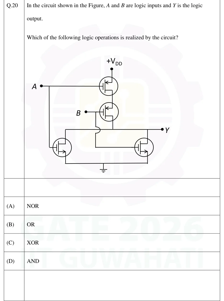
GATE 2026 EC question 20: A four-transistor CMOS gate.Tap to open full size
Figure from the GATE 2026 EC paper. It is part of the question.
Figure description

A four-transistor CMOS gate. Pull-up network: two enhancement PMOS transistors in series between +V_DD and the output node Y. The upper PMOS has its source at +V_DD and its gate driven by input A. The lower PMOS has its source on the upper PMOS's drain, its gate driven by input B, and its drain on the output line Y. Pull-down network: two enhancement NMOS transistors in parallel between Y and ground. The left NMOS has its gate on input A (a wire drops from the A input line), its drain on the Y line and its source on the common ground rail. The right NMOS has its gate on input B (a wire drops from the B input and crosses the Y line with a hop, so it is not connected to it), its drain on the Y line and its source on the common ground rail. The output Y is taken from the node where the lower PMOS drain meets both NMOS drains. The PMOS source arrows point into the channel and the NMOS source arrows point out of it.

  1. (A)

    NOR

  2. (B)

    OR

  3. (C)

    XOR

  4. (D)

    AND

Answer and solution
GATE 2026 EC Q.20: answer and solution

GATE 2026 EE Q.46

GATE 2026 · EEQ.46 · 2 marks · MCQ

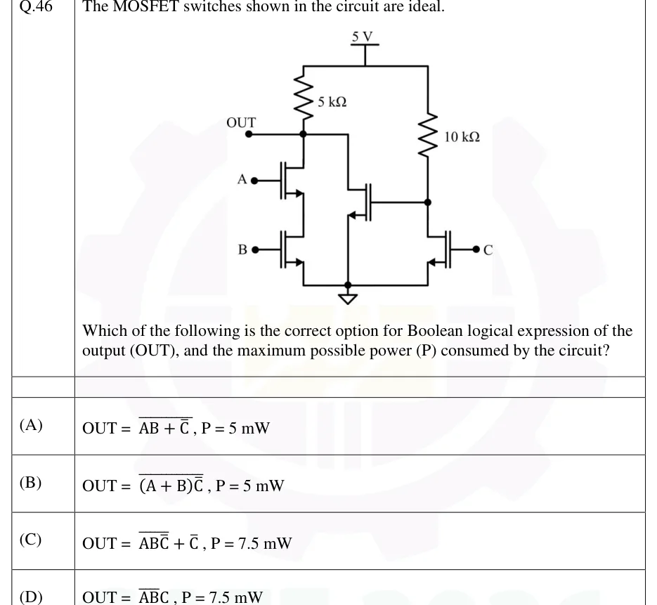
The MOSFET switches shown in the circuit are ideal.

[Figure]

Which of the following is the correct option for Boolean logical expression of the output (OUT), and the maximum possible power (P) consumed by the circuit?

GATE 2026 EE question 46: A 5 V supply feeds two resistive-load branches.Tap to open full size
Figure from the GATE 2026 EE paper. It is part of the question.
Figure description

A 5 V supply feeds two resistive-load branches. All four transistors are n-channel enhancement MOSFETs (ideal switches), and every source goes to one common ground. Left branch: a 5 kΩ resistor runs from 5 V down to node OUT, which is brought out as the output terminal. Below OUT are two NMOS in series: M_A (gate = input A) has its drain at OUT and its source tied to the drain of M_B (gate = input B), and M_B's source goes to ground. Right branch: a 10 kΩ resistor runs from 5 V down to an internal node X. NMOS M_C (gate = input C) has its drain at X and its source at ground. Middle transistor: NMOS M_X has its drain wired to node OUT, its gate wired to node X and its source at ground, so M_X is in parallel with the series pair M_A–M_B.

  1. (A)

    ,

  2. (B)

    ,

  3. (C)

    ,

  4. (D)

    ,

Answer and solution
GATE 2026 EE Q.46: answer and solution

GATE 2026 IN Q.55

GATE 2026 · INQ.55 · 2 marks · MSQ

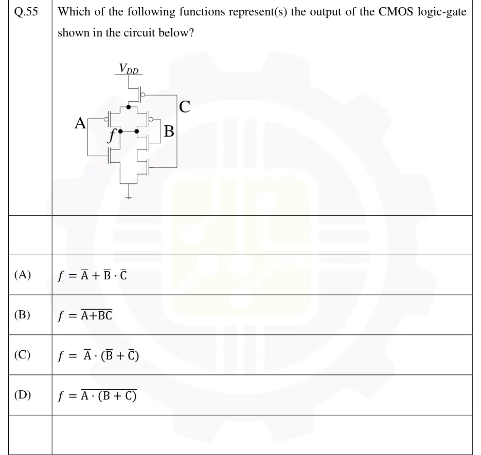
Which of the following functions represent(s) the output of the CMOS logic-gate shown in the circuit below?

GATE 2026 IN question 55: A CMOS gate between V_DD (top) and ground (bottom), with output node f at the middle.Tap to open full size
Figure from the GATE 2026 IN paper. It is part of the question.
Figure description

A CMOS gate between V_DD (top) and ground (bottom), with output node f at the middle. Pull-up network: a PMOS with gate C has its source on V_DD and its drain on an internal node X. Two PMOS transistors run in parallel from X to f: the left one has gate A and the right one has gate B. Pull-down network: two branches in parallel between f and ground. The left branch is a single NMOS with gate A (drain at f, source at ground). The right branch is an NMOS with gate B (drain at f) in series with an NMOS with gate C (source at ground). Input A drives the left PMOS and the left NMOS. Input B drives the right PMOS and the upper right NMOS. Input C drives the top PMOS and the lower right NMOS. The two PMOS drains and the NMOS drains join at the node labelled f.

  1. (A)

  2. (B)

  3. (C)

  4. (D)

Answer and solution
GATE 2026 IN Q.55: answer and solution

GATE 2022 EC Q.18

GATE 2022 · ECQ.18 · 1 mark · MCQ

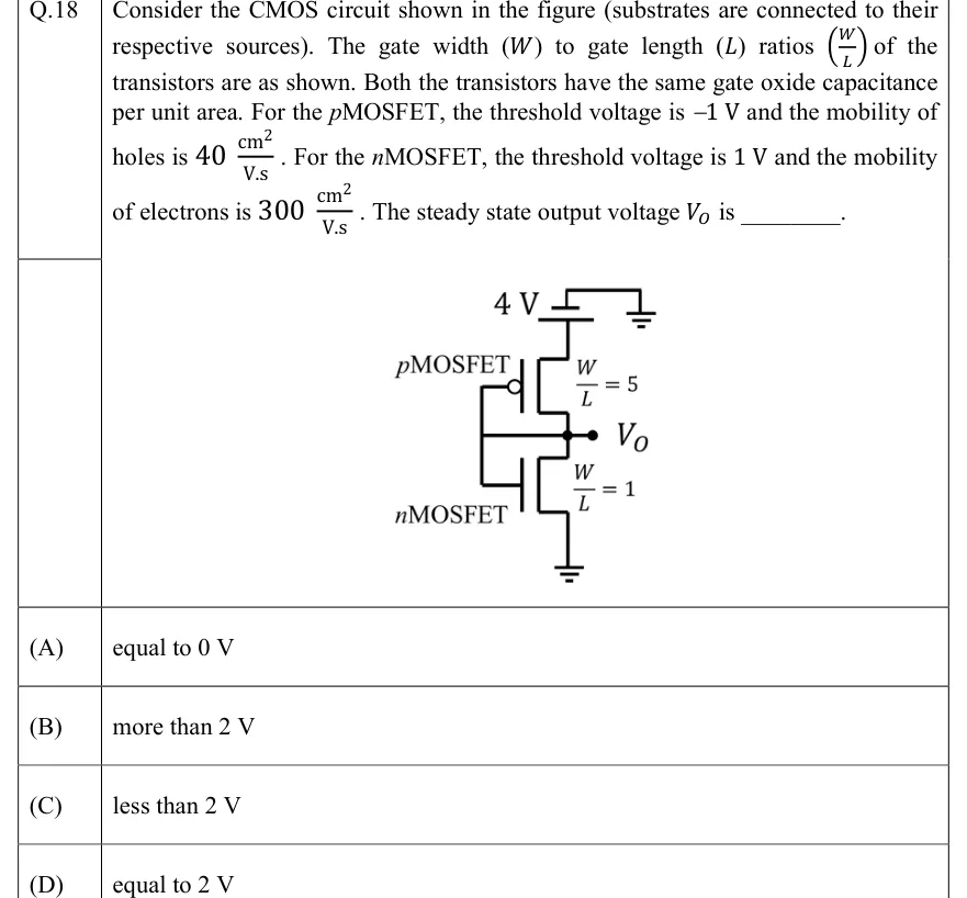
Consider the CMOS circuit shown in the figure (substrates are connected to their respective sources). The gate width () to gate length () ratios of the transistors are as shown. Both the transistors have the same gate oxide capacitance per unit area. For the MOSFET, the threshold voltage is and the mobility of holes is . For the MOSFET, the threshold voltage is and the mobility of electrons is . The steady state output voltage is ________.

GATE 2022 EC question 18: A CMOS inverter-style stack between a 4 V supply (top) and ground (bottom).Tap to open full size
Figure from the GATE 2022 EC paper. It is part of the question.
Figure description

A CMOS inverter-style stack between a 4 V supply (top) and ground (bottom). The top device is a pMOSFET (labelled pMOSFET, with the gate bubble) with W/L = 5; its source is connected to the 4 V rail. The bottom device is an nMOSFET (labelled nMOSFET) with W/L = 1; its source is connected to ground. The two drains are joined at a node that is brought out as the output V_O. The gates of the two transistors are tied together by a vertical line on the left, and this gate line is connected by a horizontal wire directly to the common drain node V_O, so the input is shorted to the output (both transistors are diode-connected). There is no separate input terminal. Substrates are tied to their respective sources.

  1. (A)

    equal to 0 V

  2. (B)

    more than 2 V

  3. (C)

    less than 2 V

  4. (D)

    equal to 2 V

Answer and solution
GATE 2022 EC Q.18: answer and solution

GATE 2022 EC Q.28

GATE 2022 · ECQ.28 · 1 mark · MSQ

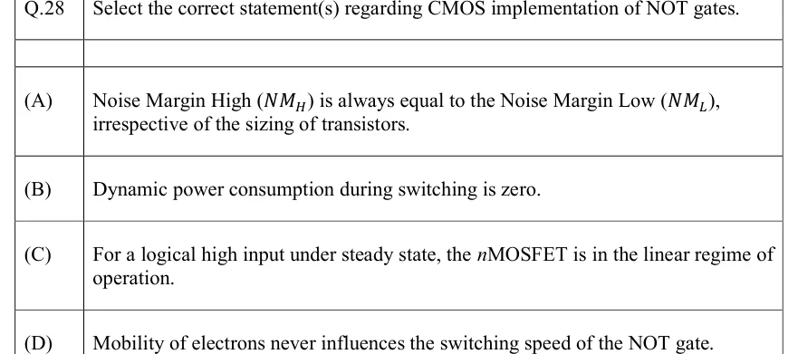
Select the correct statement(s) regarding CMOS implementation of NOT gates.

  1. (A)

    Noise Margin High () is always equal to the Noise Margin Low (), irrespective of the sizing of transistors.

  2. (B)

    Dynamic power consumption during switching is zero.

  3. (C)

    For a logical high input under steady state, the MOSFET is in the linear regime of operation.

  4. (D)

    Mobility of electrons never influences the switching speed of the NOT gate.

Answer and solution
See the question in the paper
GATE 2022 EC Q.28: answer and solution

GATE 2018 EC Q.8

GATE 2018 · ECQ.8 · 1 mark · MCQ

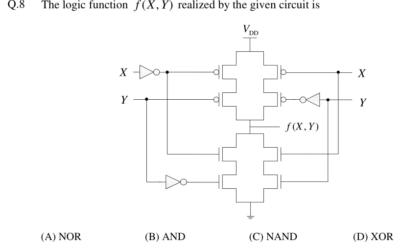
Q.8 The logic function realized by the given circuit is

GATE 2018 EC question 8: A static CMOS gate with output node f(X,Y) between a pull-up network (to V_DD) and a pull-down network (to ground).Tap to open full size
Figure from the GATE 2018 EC paper. It is part of the question.
Figure description

A static CMOS gate with output node f(X,Y) between a pull-up network (to V_DD) and a pull-down network (to ground). Input X enters on the left through an inverter, giving X; input Y enters on the left uninverted. On the right, X is taken directly, and Y goes through an inverter to give Y (Y is also tapped directly before that inverter). Pull-up network: two parallel branches from V_DD to the output, each branch two PMOS transistors in series. Left branch: upper PMOS gate = X, lower PMOS gate = Y. Right branch: upper PMOS gate = X, lower PMOS gate = Y. Pull-down network: two parallel branches from the output to ground, each branch two NMOS transistors in series. Left branch: upper NMOS gate = X (the same node as the left inverter's output), lower NMOS gate = Y (Y through a second inverter). Right branch: upper NMOS gate = X, lower NMOS gate = Y (tapped from the right-hand Y line before its inverter).

  1. (A)

    NOR

  2. (B)

    AND

  3. (C)

    NAND

  4. (D)

    XOR

Answer and solution
GATE 2018 EC Q.8: answer and solution

PRACTICE

6 questions to test yourself

PRACTICE 11 mark · MCQ

Two gate outputs are to be connected directly to one common line, so that the line is HIGH only when both outputs are HIGH (a wired-AND). Which output structure allows this?

  1. (A)

    TTL totem-pole outputs

  2. (B)

    TTL open-collector outputs with one external pull-up resistor to

  3. (C)

    Static CMOS (complementary push-pull) outputs

  4. (D)

    TTL tri-state outputs, with both gates enabled

Answer and solution

Answer: (B)

  1. Totem-pole outputs and CMOS push-pull outputs both actively drive the line HIGH. If one output is HIGH and the other LOW, the two on devices connect the supply to ground and a large current flows.

  2. Enabled tri-state outputs are ordinary push-pull outputs, so they have the same problem.

  3. An open-collector output can only pull the line down. The line is HIGH only when every output is off (HIGH), so the resistor produces the AND of the outputs.

PRACTICE 21 mark · NAT

A logic family has these worst-case levels: V, V, V and V. The noise margin of the family (the smaller of and ), in volts, is ____.

Answer and solution

Answer: (accepted range )

  1. V.

  2. V.

  3. The family's noise margin is V.

PRACTICE 32 marks · MSQ

A static CMOS gate has inputs and output . Its NMOS pull-down network, between and ground, is NMOS A in series with the parallel combination of NMOS B and NMOS C, and this whole series branch is in parallel with NMOS D. The pull-up network is the dual of the pull-down network, and no inverters are used. An overline denotes the complement. Which of the following statements are correct?

  1. (A)

  2. (B)

    The pull-up network is PMOS D in series with a branch in which PMOS A is in parallel with the series pair PMOS B and PMOS C.

  3. (C)

    The gate uses 8 transistors in total.

  4. (D)

    when , , , .

Answer and solution

Answer: (A), (B), (C)

  1. The PDN conducts when , so . A is correct.

  2. The PDN is . Its dual swaps series and parallel: in series with . B is correct.

  3. There are 4 literals, so 4 NMOS + 4 PMOS = 8 transistors. C is correct.

  4. For : , so . D is wrong.

PRACTICE 42 marks · MCQ

A CMOS inverter has V, V and V. The transconductance parameters satisfy , where . Assume the square-law model with . The switching threshold (the input voltage at which ) is

  1. (A)

    1.20 V

  2. (B)

    1.32 V

  3. (C)

    1.50 V

  4. (D)

    1.68 V

Answer and solution

Answer: (B)

  1. At both transistors are saturated: .

  2. .

  3. V.

  4. This is below because the NMOS is stronger. Option D (1.68 V) is what you get if you invert by mistake.

PRACTICE 52 marks · NAT

A CMOS logic block has gates, and each gate output drives an effective load capacitance of 20 fF. At V and a clock frequency of 1 GHz, the activity factor is , where is the probability that a gate output makes a 0-to-1 transition in a clock cycle. Neglect short-circuit and leakage power. is then lowered to 0.8 V and the clock to 800 MHz, with and the capacitances unchanged. The new dynamic power of the block, in mW, is ____.

Answer and solution

Answer: (accepted range )

  1. .

  2. Original: W.

  3. Dynamic power scales with , so the new power is W.

  4. That is 102.4 mW.

PRACTICE 61 mark · NAT

NMOS transistor M1 has its drain and its gate at V, and its source is node X. Node X drives the gate of NMOS transistor M2, whose drain is at and whose source is the output Y. Nodes X and Y each have only a capacitance to ground, and both start at 0 V. Both transistors have V. Neglect the body effect, subthreshold conduction and leakage. The final voltage at Y, in volts, is ____.

Answer and solution

Answer: (accepted range )

  1. M1 charges X until its gate-source voltage falls to , so X settles at V.

  2. M2's gate is at 1.4 V, so it charges Y until its falls to : Y settles at V.

  3. The two threshold drops add because the first transistor's output drives the second transistor's gate. If M2's gate were at instead, Y would settle at 1.4 V.

OFFICIAL GATE 2027 SYLLABUS WORDING

Copied from the GATE 2027 syllabus; see all 2027 syllabi.

GATE EC

logic gates and their static CMOS implementations

GATE IN

IC families: ECL, TTL and CMOS, CMOS implementation of logic gates

Preparing in Kolkata? IAE Academy's course for GATE ECE or GATE IN.