
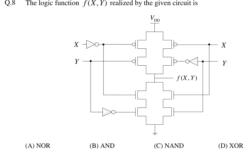
Q.8 The logic function realized by the given circuit is
 Tap to open full size
Figure description
A static CMOS gate with output node f(X,Y) between a pull-up network (to V_DD) and a pull-down network (to ground). Input X enters on the left through an inverter, giving X; input Y enters on the left uninverted. On the right, X is taken directly, and Y goes through an inverter to give Y (Y is also tapped directly before that inverter). Pull-up network: two parallel branches from V_DD to the output, each branch two PMOS transistors in series. Left branch: upper PMOS gate = X, lower PMOS gate = Y. Right branch: upper PMOS gate = X, lower PMOS gate = Y. Pull-down network: two parallel branches from the output to ground, each branch two NMOS transistors in series. Left branch: upper NMOS gate = X (the same node as the left inverter's output), lower NMOS gate = Y (Y through a second inverter). Right branch: upper NMOS gate = X, lower NMOS gate = Y (tapped from the right-hand Y line before its inverter).
- (A)
NOR
- (B)
AND
- (C)
NAND
- (D)
XOR