Conventions, half and full adders, subtractors
Conventions used in these notes. Positive logic (1 = HIGH). The complement of A is written with an overline, A. A multi-bit word is written MSB first, A=An−1…A1A0, where A0 is the LSB. Signed numbers are in 2's complement unless stated otherwise. ⊕ is XOR, ⊙ is XNOR, + is OR, and writing variables side by side means AND. Gate delays are propagation delays tpd as defined in the last section.
A combinational circuit has no memory. Every output is a Boolean function of the present inputs only, so a truth table describes it completely. A sequential circuit is different: its outputs also depend on stored state. The basic arithmetic cells are the half adder, which adds two bits, and the full adder, which adds two bits and an incoming carry. The subtractor cells work the same way but produce a borrow instead of a carry.
HALF ADDER
S=A⊕B,C=AB
Adds two 1-bit inputs and has no carry-in. A full adder with Cin=0 reduces to this.
FULL ADDER
S=A⊕B⊕Cin,Cout=AB+BCin+ACin=AB+Cin(A⊕B)
S is 1 when an odd number of the three inputs are 1. Cout is the 3-input majority function. Use the second form of Cout when the adder is built from two half adders.
HALF SUBTRACTOR (COMPUTES A − B)
D=A⊕B,Bo=AB
A borrow occurs only when the minuend A=0 and the subtrahend B=1.
FULL SUBTRACTOR (A MINUS B MINUS BORROW-IN)
D=A⊕B⊕Bin,Bout=AB+ABin+BBin=AB+Bin(A⊕B)
Computes A−B−Bin. The difference has the same expression as the full-adder sum. The borrow is the majority function of A, B and Bin. The complement goes on the minuend A.
Full adder from half adders. Two half adders and one OR gate make a full adder. The first half adder gives A⊕B and AB. The second adds Cin to A⊕B and gives S and Cin(A⊕B). ORing the two carries gives Cout.
Truth table: full adder (A plus B plus carry-in) and full subtractor (A minus B minus borrow-in)
EXAM TIP
With an odd number of inputs, an XNOR chain equals the XOR of the same inputs, so A⊙B⊙C=A⊕B⊕C and the full-adder sum can be written either way. With an even number of inputs the two differ by a complement. Minimum counts of 2-input NAND gates: 5 for a half adder, 9 for a full adder. The same counts hold for 2-input NOR gates.
EXAM TIP
Do not copy the carry expression into the borrow. The half-subtractor borrow is AB, not AB. The complement sits on the minuend, the number being subtracted from.
Multi-bit adders: ripple carry, carry look-ahead, add/subtract
An n-bit ripple-carry adder (RCA) is a chain of n full adders. The carry Ci+1 out of stage i is the carry-in of stage i+1, and C0 is the external carry-in. If there is no external carry-in, stage 0 can be a half adder. The circuit is small but slow. In the worst case a carry generated in stage 0 has to ripple through every later stage, as in 1111+0001 with C0=0.
RIPPLE-CARRY ADDER DELAY
TRCA=(n−1)tc+max(tc, ts)
tc is a stage's delay from Cin to Cout, and ts is its delay from Cin to S. Cn settles at ntc and Sn−1 at (n−1)tc+ts. The formula assumes all Ai, Bi and C0 are applied at t=0 and each stage's Ai⊕Bi is ready before its carry arrives. If stage 0 is slower from A,B than from Cin, which is the case in a gate-level full adder, compute arrival times directly (see the worked example).
A carry look-ahead adder (CLA) removes the ripple. Stage i generates a carry when Ai=Bi=1, whatever Ci is. It propagates an incoming carry when exactly one of Ai,Bi is 1. Expanding Ci+1=Gi+PiCi recursively gives every carry directly in terms of the Ps, the Gs and C0, so once the Ps and Gs are ready, all carries settle after the same two gate levels.
GENERATE, PROPAGATE, CARRY AND SUM
Gi=AiBi,Pi=Ai⊕Bi,Ci+1=Gi+PiCi,Si=Pi⊕Ci
Defining Pi=Ai+Bi gives the same carries, but then Si=Pi⊕Ci whenever Ai=Bi=1. The XOR definition lets the sum reuse Pi.
LOOK-AHEAD CARRIES (4-BIT)
C1C2C3C4=G0+P0C0=G1+P1G0+P1P0C0=G2+P2G1+P2P1G0+P2P1P0C0=G3+P3G2+P3P2G1+P3P2P1G0+P3P2P1P0C0
Each carry is a two-level SOP of P, G and C0. Ci has i+1 product terms, and the largest has i+1 literals.
CLA DELAY
tcarry=3 gate delays,tsum=4 gate delays
Measured from the operand inputs: 1 level for Pi,Gi, 2 levels (AND then OR) for every carry, and 1 XOR for every sum. This assumes every gate, XOR included, has unit delay and unlimited fan-in. The depth does not grow with n, but Cn needs (n+1)-input gates, so wide adders are built from 4-bit CLA blocks.
GROUP GENERATE AND PROPAGATE (4-BIT BLOCK)
G3:0=G3+P3G2+P3P2G1+P3P2P1G0,P3:0=P3P2P1P0,C4=G3:0+P3:0C0
G3:0=1 when the block produces a carry by itself, and P3:0=1 when it passes its carry-in straight through. A second-level look-ahead unit combines the group G and P of four blocks with the same equations as the first level, giving C4, C8, C12 and C16 without ripple.
CLA CARRY-LOGIC GATE COUNT (N BITS)
NAND=2n(n+1),NOR=n
Counts the gates that form C1…Cn from P, G and C0. Ci needs i AND gates, because its Gi−1 term needs none, plus one (i+1)-input OR gate. The count leaves out the n AND gates for G and the n XOR gates for P. For n=4: 10 AND and 4 OR.
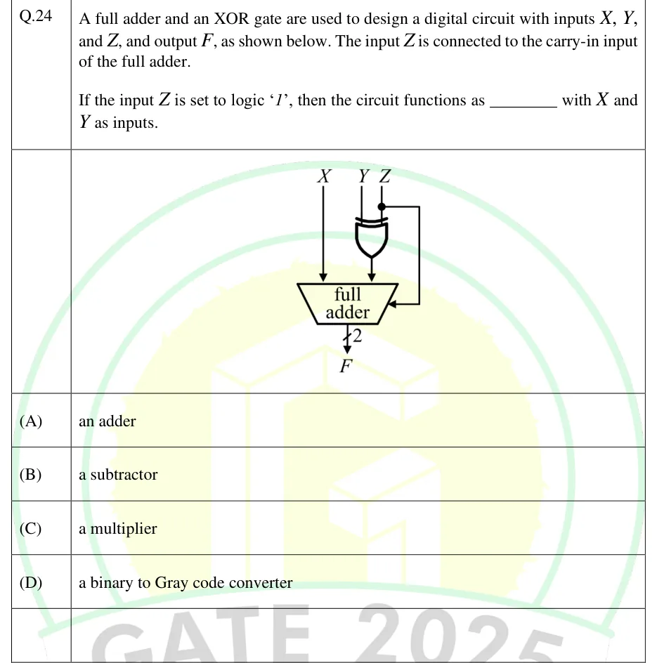
Adder–subtractor. In 2's complement, A−B=A+B+1 (modulo 2n). One n-bit adder and n XOR gates can do both operations. A mode line M is XORed with every Bi, which passes B unchanged when M=0 and inverts it when M=1. M also drives C0, which supplies the +1. Below, Yi=Bi⊕M is the operand bit that actually enters the adder.
ADDER–SUBTRACTOR
Yi=Bi⊕M,C0=M:M=0⇒A+B,M=1⇒A+B+1=A−B
Signed or unsigned operands use the same hardware. Only the reading of the flags differs.
SIGNED OVERFLOW (2'S COMPLEMENT)
V=Cn⊕Cn−1=An−1Yn−1Sn−1+An−1Yn−1Sn−1
Y=B⊕M is the operand actually entering the adder, not B itself. Overflow is possible only when both addends have the same sign, and it occurs when the sign of the sum differs from theirs.
NUMBER RANGES (N BITS)
signed: −2n−1≤x≤2n−1−1,unsigned: 0≤x≤2n−1
The sum of two n-bit unsigned numbers can need n+1 bits, because it can reach 2n+1−2.
UNSIGNED SUBTRACTION FLAG
Cn=1⟺A≥B
Applies when A−B is computed as A+B+1 on unsigned operands. Cn=0 means a borrow, and the n-bit result is then the 2's complement of B−A.
BCD ADDER CORRECTION
K=C4+Z3Z2+Z3Z1;K=1⇒add 0110, decimal carry=K
Z3Z2Z1Z0 and C4 come from a 4-bit binary adder adding two BCD digits and a carry-in. K detects binary sums of 10 to 19. The maximum sum is 9+9+1=19. A second 4-bit adder adds 0KK0 to Z3Z2Z1Z0; its own carry-out is ignored, and the decimal carry is K.
ARRAY MULTIPLIER (UNSIGNED N-BIT × M-BIT)
product width=n+m,nm AND gates,(m−1) n-bit adders
The AND gates form the partial products AiBj, and the adders sum the shifted partial-product rows. A 2-bit × 2-bit multiplier needs 4 AND gates and one 2-bit adder, which reduces to 2 half adders because nothing enters its carry-in.
WORKED EXAMPLE · RIPPLE CARRY VS CARRY LOOK-AHEAD DELAY
A 4-bit adder is built from XOR gates (4 ns), AND gates (3 ns) and OR gates (3 ns). The AND and OR delays are the same at any fan-in. Every stage forms Pi=Ai⊕Bi and Gi=AiBi, and Si=Pi⊕Ci. All operand bits and C0 arrive at t=0. Find the worst-case delay of (a) a ripple-carry adder with Ci+1=Gi+PiCi, and (b) a carry look-ahead adder that forms every carry as a two-level SOP of P, G and C0.
▸ Solution
In every stage Gi is ready at 3 ns and Pi at 4 ns.
(a) Stage 0: P0C0 is ready at 4+3=7 ns, so C1=G0+P0C0 is ready at 7+3=10 ns.
(a) In stage i≥1, Pi and Gi are already stable when Ci arrives, so each carry adds one AND and one OR: Ci+1=Ci+6 ns. That gives C2=16, C3=22, C4=28 ns.
(a) Sums: S0=P0⊕C0 at 8 ns, S1 at 14, S2 at 20, S3 at 22+4=26 ns. Worst case =max(26,28)=28 ns, set by C4.
(b) Every AND term in the look-ahead expressions contains at least one P, so the AND outputs settle at 4+3=7 ns and the ORs at 10 ns. All of C1 to C4 are ready at 10 ns.
(b) Each sum Si=Pi⊕Ci is ready at 10+4=14 ns, and so is the whole adder.
For comparison, a 16-bit ripple adder with these gates settles at 6⋅16+4=100 ns. A single-level 16-bit CLA would still take 14 ns but needs 17-input gates.
Answer: (a) Ripple carry: 28 ns, set by C4 (S3 is ready at 26 ns). (b) Carry look-ahead: 14 ns, set by the sums (the carries are ready at 10 ns).
EXAM TIP
Overflow and carry mean different things. For unsigned addition the carry-out Cn is the overflow. For signed 2's-complement addition, use V=Cn⊕Cn−1 and ignore Cn. Adding two numbers of opposite sign can never overflow.
EXAM TIP
When a question gives gate delays, draw each stage and write an arrival time at every node. Stage 0 often has a different delay from the others, because its carry path starts at A0,B0 through an XOR. The later stages all add the same Cin→Cout delay.
Comparators, parity generators and code converters
A magnitude comparator decides whether A>B, A=B or A<B for unsigned words. It scans from the MSB down: the most significant bit position in which the two words differ decides the result.
1-BIT COMPARATOR
(A>B)=AB,(A<B)=AB,(A=B)=A⊕B
Exactly one of the three outputs is 1 for any input.
4-BIT MAGNITUDE COMPARATOR
xi(A>B)(A<B)=Ai⊕Bi,(A=B)=x3x2x1x0=A3B3+x3A2B2+x3x2A1B1+x3x2x1A0B0=A3B3+x3A2B2+x3x2A1B1+x3x2x1A0B0
Unsigned operands, with A3 and B3 as the MSBs. xi=1 when bit i of the two words is equal.
A parity generator appends one bit so that the transmitted word has an even number of 1s (even parity) or an odd number (odd parity). The checker at the receiver XORs all the received bits, parity bit included.
PARITY GENERATOR
PE=Dn−1⊕⋯⊕D1⊕D0,PO=PE
PE makes the total count of 1s in data plus parity even. PO makes it odd.
PARITY CHECKER
E=P⊕Dn−1⊕⋯⊕D0
In an even-parity system, E=1 flags an error. In an odd-parity system, E=0 flags one. The check detects any odd number of bit errors, misses any even number, and cannot locate the bit in error.
A code converter is a multi-output combinational circuit. Write the truth table from input code to output code, mark unused input combinations as don't-cares, and minimise each output bit. Binary↔Gray conversion needs only XOR gates. A BCD-to-7-segment decoder has 4 inputs, 7 outputs (segments a to g) and 6 don't-care inputs (1010 to 1111). On a common-cathode display a segment lights when driven with 1, so the outputs are active-high. On a common-anode display it lights when driven with 0, so every output is complemented.
BINARY TO GRAY
Gn−1=Bn−1,Gi=Bi+1⊕Bi(i=n−2,…,0)
This is the same as XORing the binary word with a copy of itself shifted right by one place. Needs n − 1 XOR gates, all working in parallel.
GRAY TO BINARY
Bn−1=Gn−1,Bi=Bi+1⊕Gi=Gn−1⊕Gn−2⊕⋯⊕Gi
Each binary bit is the running XOR of the Gray bits from the MSB down. Built as a chain, the delay is up to n − 1 XOR delays.
BCD TO EXCESS-3
E3E2E1E0=B3B2B1B0+0011
Applied to each BCD digit, valid for digits 0 to 9. Excess-3 is self-complementing: complementing every bit of a digit's Excess-3 code gives the Excess-3 code of its 9's complement.
BCD TO 7-SEGMENT, SEGMENT A
a=B3+B1+B2B0+B2B0
Input B3B2B1B0 is 8421 BCD with B3 the MSB. Segments are active-high and 1010 to 1111 are don't-cares. Segment a is off only for digits 1 and 4. This assumes 6 is drawn with segment a.
Codes for the decimal digits. Segments: a top, b upper right, c lower right, d bottom, e lower left, f upper left, g middle. 6 is drawn with a, 9 with d, and 7 without f.
EXAM TIP
The two Gray conversions run in opposite directions. Binary to Gray XORs neighbouring binary bits. Gray to binary XORs each Gray bit with the binary bit just found above it, not with the next Gray bit. In the full n-bit reflected Gray code, consecutive codes differ in exactly one bit, and so do the last and first of all 2n codes. A shortened list is not cyclic: in the table above, 9 (1101) and 0 (0000) differ in three bits.
Multiplexers and demultiplexers
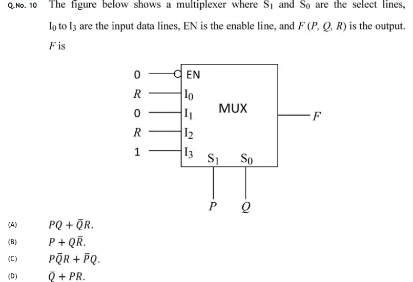
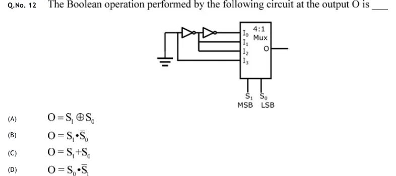
A 2n:1 multiplexer (data selector) has 2n data inputs I0…I2n−1, n select lines Sn−1…S0 and one output. Sn−1 is the MSB of the select code, and Ik reaches the output when the select code equals k. In AND–OR form it uses 2n AND gates with n+1 inputs each, one OR gate with 2n inputs, and n inverters for the complemented select lines. A demultiplexer works the other way: it routes one data input D to one of 2n outputs.
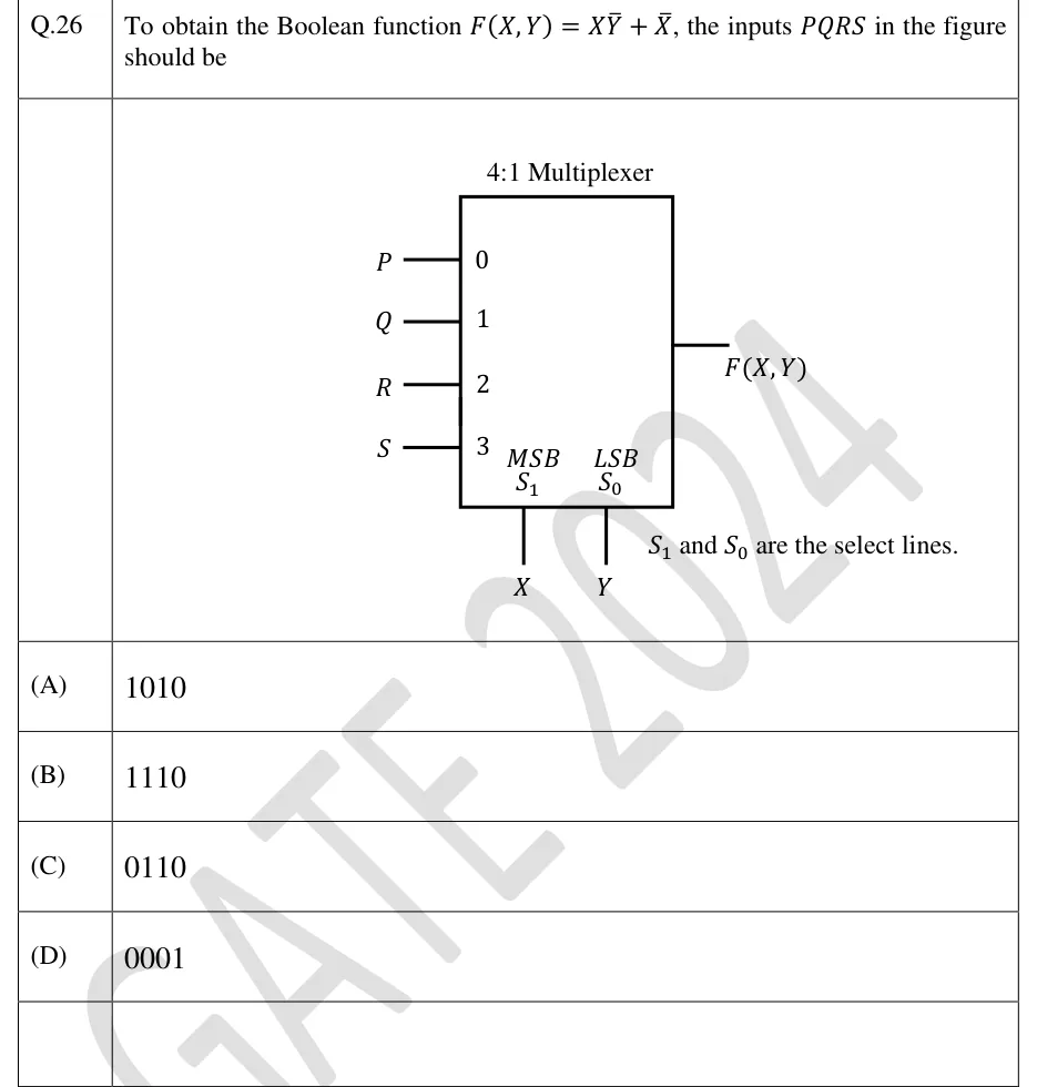
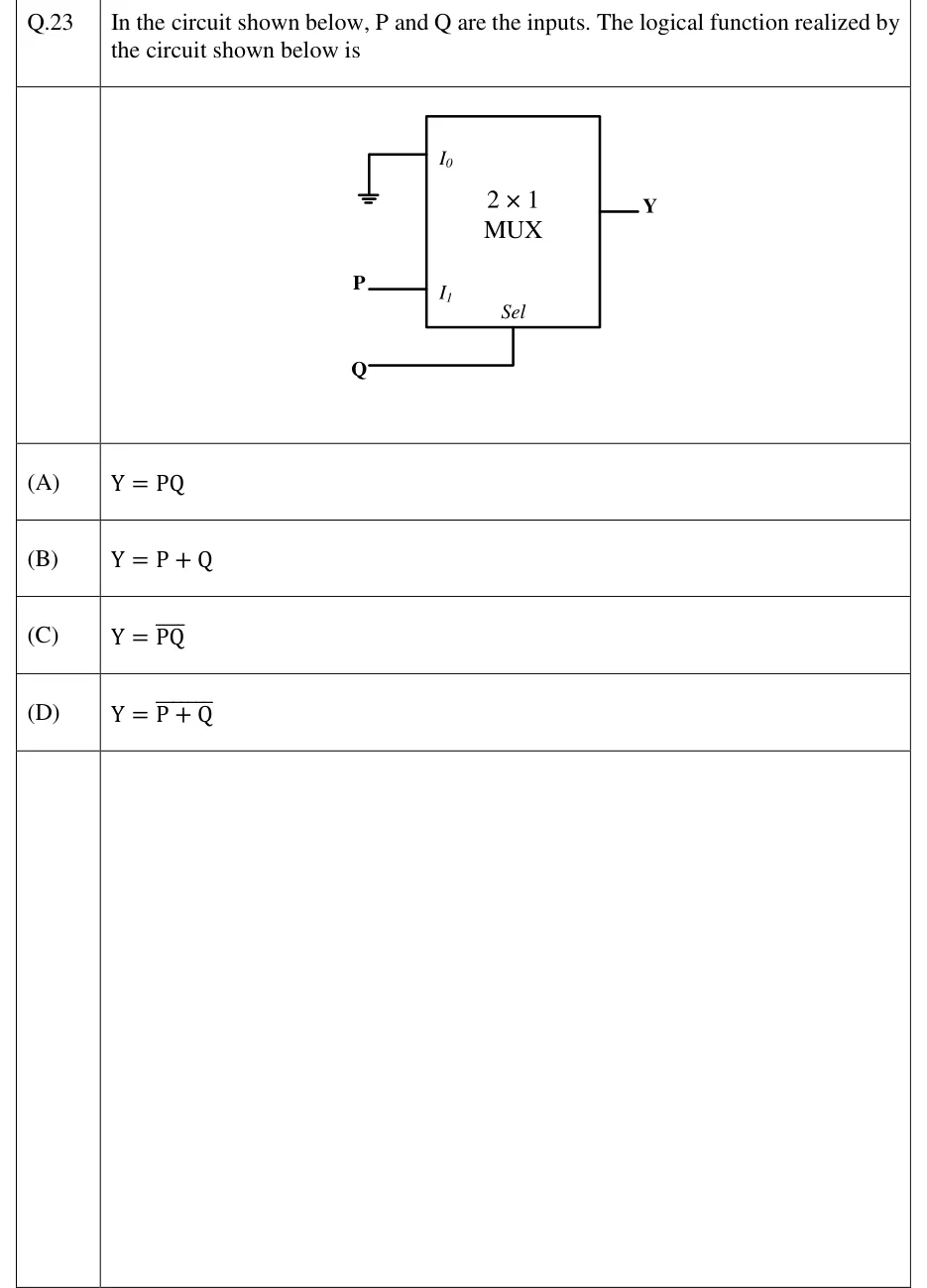
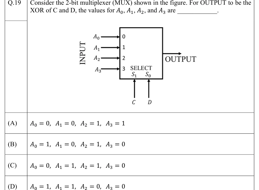
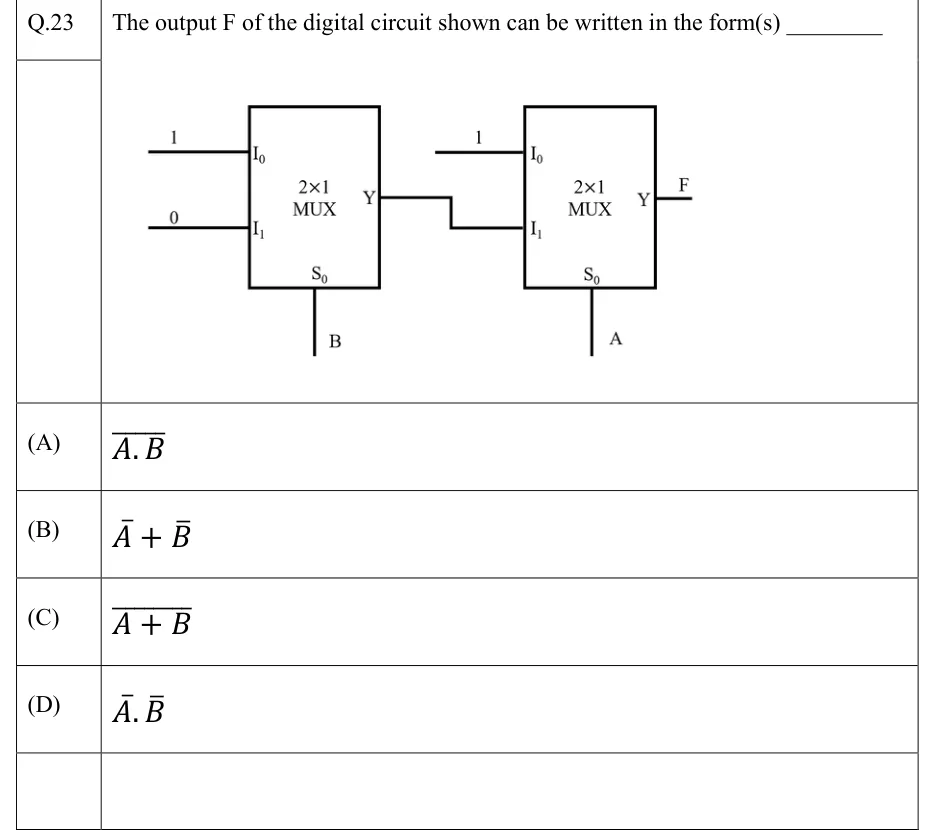
2:1 AND 4:1 MUX
Y2:1=SI0+SI1,Y4:1=S1S0I0+S1S0I1+S1S0I2+S1S0I3
S1 is the MSB of the select code.
GENERAL MUX WITH N SELECT LINES
Y=k=0∑2n−1mkIk
mk is the k-th minterm of the select variables and ∑ means OR. An enable input E, where present, multiplies the whole expression.
DEMUX WITH N SELECT LINES
Yk=mk⋅D,k=0,1,…,2n−1
mk is the k-th minterm of the select lines. A 1:2n DEMUX is the same circuit as an n-to-2n decoder whose enable input carries the data.
MUX TREE
NMUX=⌈k−1N−1⌉(k:1 MUXes to build an N:1 MUX)
N and k are powers of 2. Each k:1 MUX cuts the number of candidate signals by at most k − 1. When N is a power of k the division is exact and the MUXes form a full tree: 16:1 from 4:1 needs 4 + 1 = 5, 8:1 from 2:1 needs 7, 64:1 from 4:1 needs 21. Otherwise the last MUX has unused inputs: 32:1 from 4:1 needs 8 + 2 + 1 = 11. The same count holds for a 1:N DEMUX built from 1:k DEMUXes.
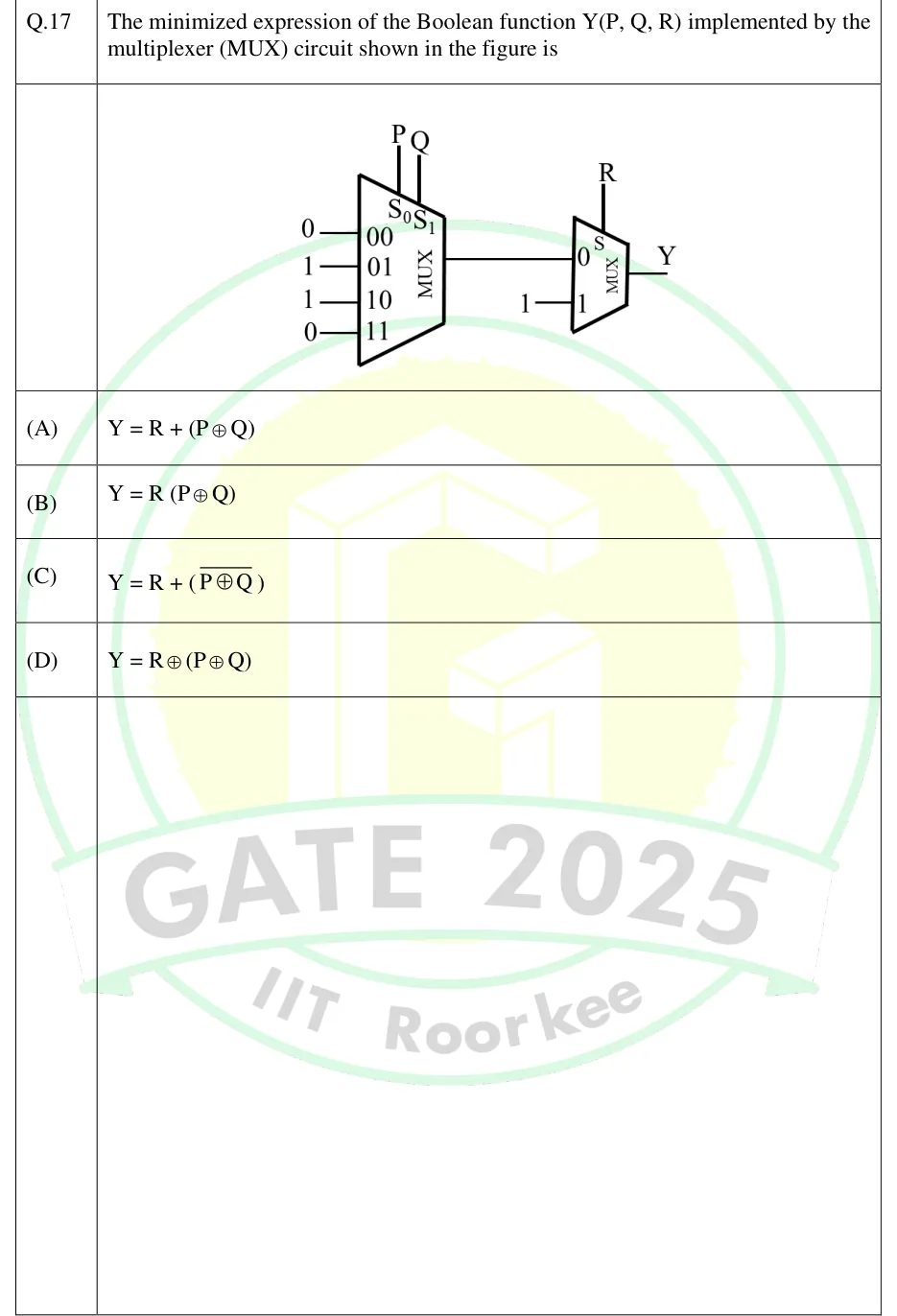
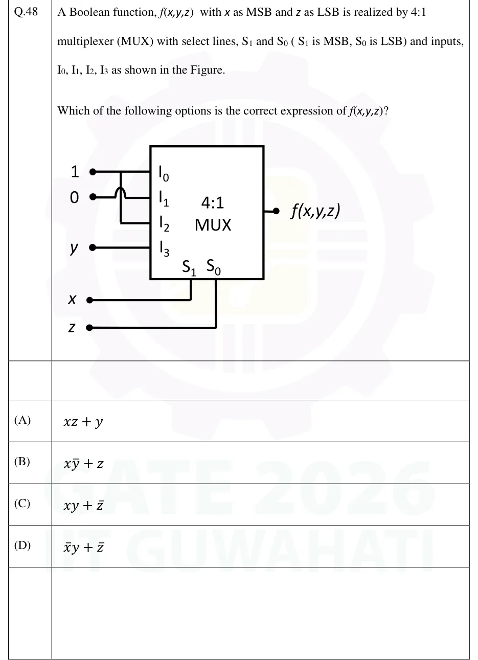
Because the output is ∑mkIk, a 2n:1 MUX with only 0 and 1 on its data inputs implements any function of its n select variables: the data inputs are simply the truth-table column. If the data inputs can also take one more variable or its complement, the MUX implements any function of n+1 variables. So an n-variable function needs only a 2n−1:1 MUX.
Implementing an n-variable function on a MUX with n − 1 select lines
Put n−1 of the variables on the select lines, keeping their order: the most significant of them goes on the highest select line. Call the remaining variable X.
For each select code k, find the two minterms of F that share it. They differ only in X. If X is the LSB they are m2k (X=0) and m2k+1 (X=1). If X is the MSB they are mk (X=0) and mk+2n−1 (X=1).
Set Ik=0 if neither minterm is in F, 1 if both are, X if only the one with X=1 is, and X if only the one with X=0 is.
For any other choice of X, or as a check, use an implementation table: two rows (X=0 and X=1), one column per data input, and every minterm written in the cell for its own X value and select code. Mark the minterms of F and read each column by the rule above.
Set don't-care minterms to 0 or 1, whichever makes a data input a constant.
WORKED EXAMPLE · A 4-VARIABLE FUNCTION ON AN 8:1 MUX
Implement F(A,B,C,D)=∑m(1,3,4,11,12,13,14,15) with an 8:1 MUX. Use S2S1S0=ABC (A is the MSB) and put D, D, 0 or 1 on the data inputs.
▸ Solution
With S2S1S0=ABC, input Ik is selected when ABC=k. The two minterms sharing that code are m2k (D=0) and m2k+1 (D=1).
k=0: m0∈/F, m1∈F, so I0=D. k=1: m2∈/F, m3∈F, so I1=D.
k=2: m4∈F, m5∈/F, so I2=D. k=3: m6,m7∈/F, so I3=0.
k=4: m8,m9∈/F, so I4=0. k=5: m10∈/F, m11∈F, so I5=D.
k=6: m12,m13∈F, so I6=1. k=7: m14,m15∈F, so I7=1.
Spot check: ABCD=0100 (m4) selects I2=D=1, which is correct. ABCD=0101 (m5) gives D=0, also correct.
Answer: I0=D, I1=D, I2=D, I3=0, I4=0, I5=D, I6=1, I7=1. One inverter supplies D.
EXAM TIP
A 2:1 MUX is functionally complete when the constants 0 and 1 are available. NOT: S=A, I0=1, I1=0 gives A. AND: S=A, I0=0, I1=B gives AB. OR: S=A, I0=B, I1=1 gives A+B. XOR needs a complemented input: S=A, I0=B, I1=B.
EXAM TIP
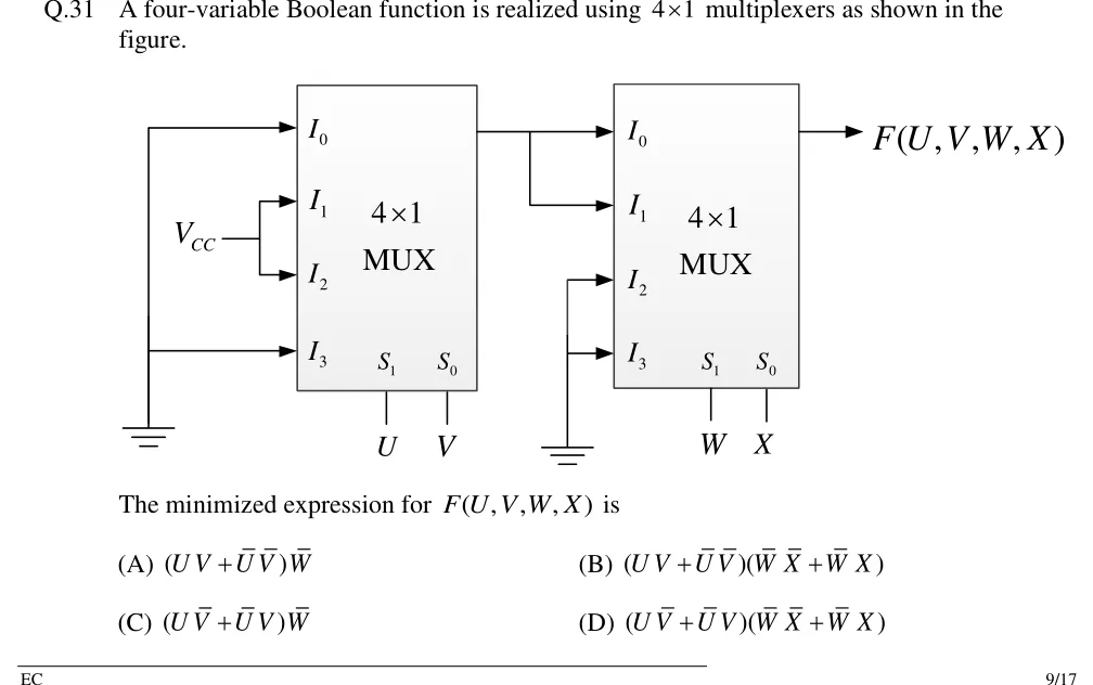
Check which variable drives which select line before you read off minterms. If the circuit puts the first-listed variable on S0 instead of the highest select line, the index k changes and the minterm list comes out wrong. For cascaded MUXes, write each MUX's output as an expression, then substitute it into the next.
Decoders and encoders
An n-to-2n decoder activates exactly one of its 2n outputs: output k is active when the input code equals k. With active-high outputs, each output is a minterm of the inputs. A decoder plus OR gates therefore implements any set of functions of its inputs in sum-of-minterms form, with one decoder shared by all of them. An enable input E gates every output. A decoder with an enable is the same circuit as a 1:2n demultiplexer, with E as the data input and the code inputs as the select lines. Internally it uses 2n AND gates with n inputs each (n+1 with an enable), plus n inverters.
DECODER OUTPUTS
Yk=E⋅mk (active-high),Yk=E⋅mk (active-low)
mk is the k-th minterm of the inputs. With E=1, an active-low output is the maxterm Mk=mk.
FUNCTION FROM A DECODER
F=k∈F∑Yk(active-high outputs, OR gate)=k∈F∏Yk(active-low outputs, NAND gate)=k∈/F∏Yk(active-low outputs of the 0-minterms, AND gate)
The decoder must be enabled. ∑ means OR, ∏ means AND, and Yk is the active-low output line. A NOR gate on the active-high outputs of the 0-minterms also gives F. Use the 0-minterm form when F has more 1s than 0s, because the gate then needs fewer inputs.
DECODER TREE
Ndec=k−1N−1(decoders with k outputs to build N outputs)
Valid when N is a power of k and each decoder has an enable input. Example: a 4:16 decoder from 2:4 decoders needs 4 + 1 = 5, with the first-level decoder driving the enables. A 3:8 decoder needs only two 2:4 decoders: the MSB drives one enable directly and the other through an inverter.
An encoder does the reverse job: it has 2n inputs and n outputs that give the index of the active input. A plain encoder assumes exactly one input is active. A priority encoder outputs the index of the highest-priority active input. It also has a valid output V, because otherwise 'input 0 active' and 'no input active' both give code 0.
8:3 ENCODER (OCTAL TO BINARY)
Y2=D4+D5+D6+D7,Y1=D2+D3+D6+D7,Y0=D1+D3+D5+D7
Valid only when exactly one input is 1. D0 does not appear, so 'D0 active' and 'no input active' both give 000.
4:2 PRIORITY ENCODER (D3 HIGHEST PRIORITY)
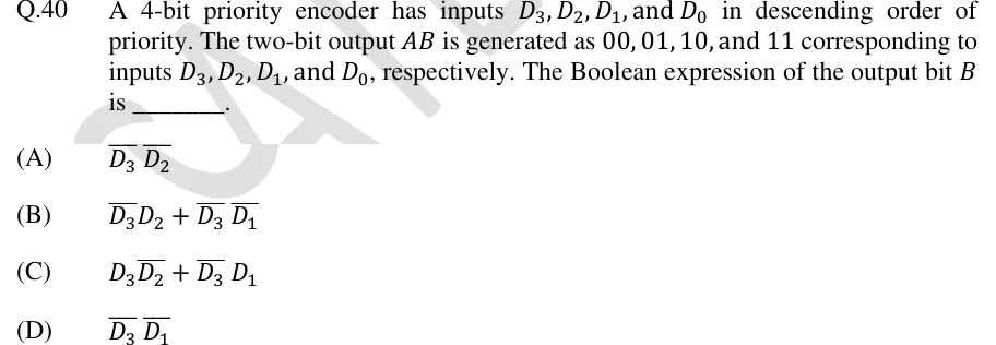
Y1=D3+D2,Y0=D3+D2D1,V=D3+D2+D1+D0
Active-high inputs and outputs. V=0 means no input is active, and Y1Y0 should then be ignored.
EXAM TIP
A plain encoder with two active inputs outputs the bitwise OR of their codes. For example, D3 and D5 together give 011+101=111, which looks the same as D7 alone. A priority encoder avoids this.
EXAM TIP
Before choosing the output gate, check whether the decoder outputs are active-low. Active-low outputs are maxterms, so ORing them does not give F. A NAND of the 1-minterm lines does, and so does an AND of the 0-minterm lines.
ROM, PLA, PAL and the critical path
A ROM with n address lines and m data outputs is a combinational circuit. It is a fixed n-to-2n decoder (the AND array, which produces every minterm) followed by a programmable OR array. The ROM stores the truth table directly, so no minimisation is needed and it can hold any m functions of n variables.
ROM SIZE
ROM size=2n×m bits
n is the number of input variables (address lines) and m the number of output functions (word length). All 2n words count, even if some input combinations never occur.
A PLA has a programmable AND array, which forms k product terms from any inputs or their complements, and a programmable OR array, in which each output ORs any of the k terms. Outputs can share product terms, so minimise the outputs together to reduce the number of distinct terms. A PAL has a programmable AND array but a fixed OR array. Each output owns a fixed number of product terms and cannot share them.
PLA PROGRAMMABLE CONNECTIONS
Nlinks=2nk+km
For n inputs, k product terms and m outputs. The AND array connects each term to any of the 2n true and complemented literals; the OR array connects each output to any term. Add m if each output has a programmable inverter.
ROM vs PLA vs PAL
| | | | |
|---|
| | | All 2n minterms, no minimisation | Dense truth tables, look-up tables, code converters |
| | | k chosen terms, shared among outputs | Many outputs that share product terms |
| | | Fixed number per output, not shared | Each output needs only a few terms |
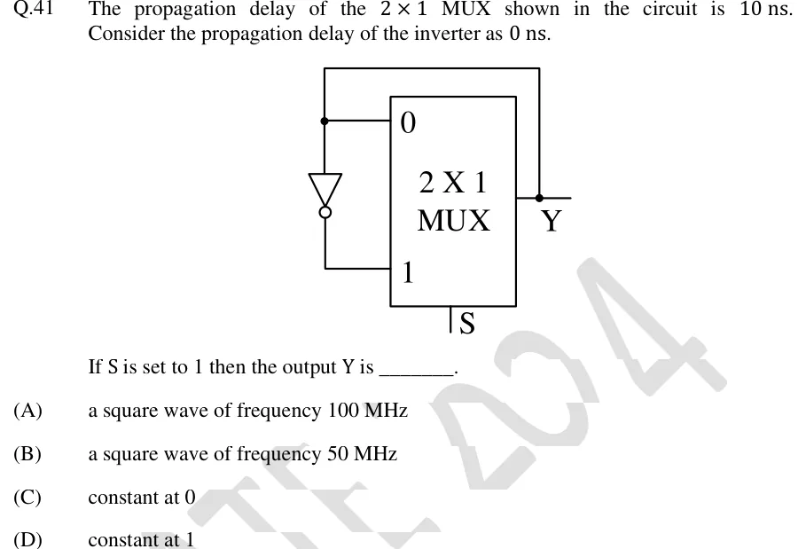
Propagation delay tpd of a gate is taken here as the worst-case time from an input change until the output settles, the larger of tPLH and tPHL. Some data sheets quote the average of the two, so use whichever definition the question gives. The critical path is the input-to-output path with the largest total delay. The circuit's outputs are valid only that long after the last input change.
ARRIVAL TIME AND CIRCUIT DELAY
tout=imax(tin,i)+tpd,T=outputsmaxtout
Apply this gate by gate from the inputs to the outputs. T is the delay along the longest path.
Finding the critical path
Give each primary input its arrival time: 0 unless stated. If complements are not available, add an inverter delay to each complemented input.
Work from the inputs towards the outputs. Each gate's output time is the latest of its input times plus that gate's tpd.
The largest time at any primary output is the circuit delay.
To find the critical path, trace back from that output, at each gate following the input that set the maximum.
Static hazards. Because paths have unequal delays, an output can glitch during an input change even when its final value equals its starting value. In a two-level AND–OR (SOP) circuit a static-1 hazard can occur when a single input change moves between two 1-cells of the K-map that no single product term covers. Adding the redundant consensus term that covers both cells removes it. Example: F=AB+AC can dip to 0 when A changes while B=C=1; adding BC holds F at 1 throughout.
EXAM TIP
ROM size counts every address, don't-cares included. A BCD-to-7-segment converter stored in ROM needs 24×7=112 bits, even though only 10 addresses are used. In a PLA, a product term shared by two outputs counts only once.
EXAM TIP
Two-level AND–OR logic has a delay of 2 gate levels when complemented inputs are available, and 3 when inverters must be added. A NAND–NAND realisation has the same structure and depth as AND–OR.

 Tap to open full size