GATE 2026 IN Q.23
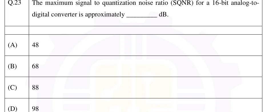
The maximum signal to quantization noise ratio (SQNR) for a 16-bit analog-to-digital converter is approximately _________ dB.
- (A)
48
- (B)
68
- (C)
88
- (D)
98

GATE EC · EE · IN
Sample-and-hold circuits, DACs and ADCs link analog signals to digital logic. An S/H freezes the input, an ADC turns it into an n-bit code, and a DAC turns a code back into a voltage or current. Calculations in this topic come down to picking the right result and the right resolution convention: step size, DAC output for a code, comparator count, conversion time, the SAR bit sequence, dual-slope counts, droop, SQNR or ENOB. So the notes give every formula with its conditions.
18 previous-year questions · 18 solved · 6 practice questions
An ADC maps a continuous input voltage to one of output codes. A DAC maps an -bit code back to one of output levels. The gap between adjacent levels is the step size , also called one LSB (least significant bit). Almost every calculation in this topic starts from .
Conventions used throughout these notes.
DECIMAL VALUE OF A CODE
Straight binary. The MSB has weight and the LSB has weight 1.
STEP SIZE (RESOLUTION IN VOLTS)
Convention used in these notes: is the full-scale range, i.e. the reference span. For a bipolar range to , .
IDEAL DAC OUTPUT
Ideal (zero offset, linear) straight-binary DAC. Magnitude only. An inverting op-amp output stage adds a minus sign.
FULL-SCALE (ALL-ONES) OUTPUT
The largest output the converter actually produces, one LSB below .
PERCENTAGE RESOLUTION
The step as a fraction of the full-scale (all-ones) output. Some problems use instead, meaning the step as a fraction of . Check which one the question defines.
MINIMUM NUMBER OF BITS FOR A REQUIRED RESOLUTION
From , where is the largest step allowed. If the question instead fixes the full-scale (all-ones) output , the condition is .
IDEAL ADC OUTPUT CODE (TRUNCATING)
For a converter whose code changes at integer multiples of , e.g. an SAR that keeps a bit when . Inputs at or above give the all-ones code . A rounding converter has its thresholds shifted down by , so , clamped to .
EXAM TIP
The versus trap. If a question gives the reference or the full-scale range, use . If it gives the full-scale output, meaning the output for the all-ones code, use . For 8 bits and 10 V these give 39.06 mV and 39.22 mV, so a question may list both values as options.
Bipolar converters. For a range of to , . The code is either offset binary (all zeros means and means 0 V) or 2's complement. 2's complement is offset binary with the MSB inverted. These notes use 2's complement for signed codes unless stated.
BIPOLAR DAC OUTPUT (RANGE −V_R TO +V_R)
is the unsigned value of an offset-binary code, and is the signed value of a 2's-complement code. For the same output, . The range is (offset binary , 2's complement ) to (offset binary , 2's complement ).
An ADC that compares the input more than once during a conversion (SAR, counter-type) needs its input held constant, to within LSB, for the whole conversion. A sample-and-hold (S/H) is an analog switch (a MOSFET or CMOS transmission gate) that charges a hold capacitor . A high-input-impedance buffer (an op-amp voltage follower) follows the capacitor.
A flash ADC can work without a separate S/H, because its clocked comparators all latch at the same instant, and that latching does the sampling. An integrating (dual-slope) ADC measures the average of the input over its fixed integration time, so it does not need an S/H either.
S/H specifications (definitions)
Acquisition time : the time from the sample command until the capacitor voltage reaches, and stays within, a stated error band of the input, for example LSB for a full-scale step.
Aperture time : the delay from the hold command to the moment the switch actually opens. A fixed delay can be cancelled by issuing the command earlier. Its random variation, the aperture uncertainty (jitter) , cannot be cancelled, and it limits the input frequency.
Droop: in hold mode, leakage current (switch off-leakage, buffer bias current, capacitor leakage) charges or discharges . The held voltage drifts at the rate .
Hold step (pedestal): the switch injects charge into as it opens, causing a step of .
Feedthrough: in hold mode the input still couples to through the switch's off-capacitance.
Hold settling time: the time after the hold command for the output to settle within the error band.
ACQUISITION TIME (RC CHARGING)
is the allowed error as a fraction of the step, and is the source resistance. Assumes single-pole RC settling with no slew-rate limit.
ACQUISITION TIME TO WITHIN ±1/2 LSB
Full-scale step in an -bit system. Setting , i.e. half an LSB of full scale, in the formula above gives this. Same assumptions: single-pole RC settling, no slew-rate limit.
HOLD-MODE DROOP
is the total leakage current at the hold capacitor. To keep droop over a conversion time within LSB, choose .
HOLD STEP (PEDESTAL)
is the charge the switch injects into as it opens.
APERTURE-JITTER LIMIT ON INPUT FREQUENCY
An input has maximum slope , and the error (slope ) must stay within LSB. The right-hand form is for a full-scale sine, .
INPUT-FREQUENCY LIMIT WITH NO S/H
With no S/H, a full-scale sine (peak-to-peak ) must change by less than LSB during the whole conversion time . The derivation is the same as above, with in place of . A criterion of 1 LSB instead of LSB doubles this limit, so use the criterion the question states.
SAMPLING THEOREM
For a signal band-limited to . is the Nyquist rate. Sampling at exactly that rate can fail for a component at , whose samples may all fall on its zeros. An anti-aliasing low-pass filter before the S/H enforces the band limit.
APPARENT (ALIAS) FREQUENCY AFTER SAMPLING
A sinusoid at sampled at gives the same samples as one at , which lies between 0 and . If , then and there is no aliasing.
EXAM TIP
is a trade-off. A larger gives less droop and a smaller pedestal. It also gives a longer acquisition time, since , and needs more drive current. With single-pole settling, if a question halves droop by doubling , doubles as well.
Analog front end (data-acquisition chain). When many sensor channels share one converter, an analog multiplexer connects one channel at a time to a common S/H and ADC. The MUX is an array of CMOS switches with a channel-address decoder. Its key specifications are on-resistance, off-isolation (feedthrough from an off channel to the output), channel-to-channel crosstalk, switching time and settling time after a channel change. If channels are scanned in turn at a total rate , each channel is sampled at .
A programmable-gain amplifier (PGA) sits after the MUX and has a digitally selected gain, for example 1, 2, 4, …, 128. It scales a small channel up to fill the ADC range, which makes the quantisation step referred to the input smaller.
PER-CHANNEL SAMPLE RATE OF A MULTIPLEXED ADC
For channels scanned in equal turns by one ADC running at conversions per second.
INPUT-REFERRED LSB WITH PGA GAIN G
Valid while (peak input) stays within the ADC range. Beyond that, the ADC saturates.
Order of a typical multichannel acquisition chain
Sensor or transducer
Signal conditioning (amplification, level shift, isolation)
Anti-aliasing low-pass filter (one per channel, before the MUX)
Analog multiplexer
Programmable-gain amplifier
Sample-and-hold
ADC
Digital processor or interface
WORKED EXAMPLE
A sample-and-hold drives a 10-bit ADC with V. The hold capacitor is nF and the switch on-resistance is (source resistance negligible). The total hold-mode leakage current is 5 nA and the ADC's conversion time is s. Find (a) the acquisition time for a full-scale step to settle within LSB, (b) the droop during one conversion, and (c) the highest full-scale sine frequency that can be sampled if the aperture jitter is 1 ns and the jitter error must stay within LSB.
mV, so LSB mV.
(a) s ns. Settling to LSB of a full-scale step needs , so ns.
(b) V. That is 1% of the 5 mV budget, so droop is not a problem.
(c) kHz.
Answer: (a) s; (b) V, well inside LSB = 5 mV; (c) kHz.
Weighted-resistor DAC. Each bit drives a resistor into the virtual ground of an inverting op-amp summer with feedback resistor . Bit uses the resistor , so the MSB gets the smallest resistor () and the LSB the largest (). The branch currents are therefore binary-weighted, and the op-amp turns their sum into a voltage.
WEIGHTED-RESISTOR DAC OUTPUT
MSB resistor , LSB resistor . Bit 1 connects its resistor to and bit 0 to ground. Ideal op-amp. With this reduces to .
Its weakness is the resistor spread: an -bit design needs different values spanning , which is 128 : 1 for 8 bits. Such wide ratios are hard to make and to match on a chip.
The design is therefore practical only for a few bits.
R-2R ladder DAC. It uses only two values, and . At every node, the leg and the rest of the ladder toward the LSB end both present . So current arriving at a node splits equally, and the reference sees a total of .
In the common current-mode (inverting) form, the reference drives the ladder. Each leg is switched to the op-amp's virtual ground (bit 1) or to ground (bit 0). Both are at 0 V, so the ladder currents never change with the code. The reference always supplies . The MSB leg carries , the next , and so on down to in the LSB leg.
R-2R LADDER DAC OUTPUT (CURRENT MODE, INVERTING)
Legs switched between virtual ground (bit 1) and ground (bit 0). Ideal op-amp. With : , and the step is .
R-2R LEG CURRENT FOR BIT K
MSB (): . LSB (): . The current drawn from the reference, , is the same for every code.
R-2R LADDER, VOLTAGE MODE (OPEN CIRCUIT)
Each leg is switched between (bit 1) and ground (bit 0), and the LSB end is terminated in to ground. The output is the open-circuit voltage at the MSB node, where the Thevenin resistance is for every code.
Current-steering DAC. An array of matched current sources, each switched by a differential pair to either the output node or a dump node. The sources stay on all the time and only their current is redirected, so switching is fast. This is the usual high-speed architecture. The sources come in three arrangements:
The output current drives a load resistor or a transimpedance amplifier.
A multiplying DAC is a DAC (usually R-2R) whose reference is a varying analog signal. Its output is , so it acts as a digitally controlled attenuator.
CURRENT-STEERING DAC OUTPUT
is the unit (LSB) current. The second form applies when the output drives a load resistor .
Property | Weighted-resistor | R-2R ladder | Current-steering |
|---|---|---|---|
Resistor values | values, to | Two: and | Matched current sources (unit cells) |
Number of resistors (excluding ) | ( legs of , series , one termination) | Not resistor-based | |
Spread of values | Binary ; unary 1 : 1 | ||
Current from reference | Varies with code | Constant, (current mode) | Sources always on, current redirected |
Typical use | A few bits | Medium resolution, easy to integrate | High-speed conversion |
WORKED EXAMPLE
An 8-bit current-mode R-2R ladder DAC has V, k and a feedback resistor k on an ideal inverting op-amp. Find the step size, the output for the input (MSB first), the full-scale output, the percentage resolution, and the current in the MSB leg when .
With : , and the step is mV.
, so V.
Full scale is code 11111111, : V, one LSB short of V.
Percentage resolution of the full-scale output.
MSB leg current mA. The reference always supplies mA, whatever the code.
Answer: mV; V; full scale V; resolution 0.392 %; mA.
EXAM TIP
Monotonic DAC: the output never decreases when the code increases. This is guaranteed when every step is positive, i.e. DNL LSB at every code. In a binary-weighted DAC the worst case is the major transition . Every bit switches there, so the MSB's error is compared with the sum of all the others.
EXAM TIP
To check a weighted-resistor or R-2R answer, add the branch currents directly. Each bit equal to 1 contributes into the virtual ground, and . This works even when a question uses non-standard resistors or a non-standard .
Flash (parallel) ADC. A resistor string divides into threshold voltages. Each threshold feeds one comparator, whose other input is . Every comparator whose threshold is below the input reads 1, which gives a thermometer code, and a priority encoder converts this to -bit binary. A conversion takes one comparator delay plus the encoder delay, so flash is the fastest type. The comparator count, and with it the area and power, roughly doubles with each extra bit.
A two-step (half-flash, subranging) ADC first digitises the MSBs with a coarse flash. It then subtracts the DAC value of that result from the input and digitises the remainder with a second flash. For bits split equally this needs comparators, e.g. 30 instead of 255 for 8 bits.
FLASH ADC COMPARATORS AND LADDER RESISTORS
With thresholds at integer multiples of the ladder uses equal resistors. A rounding ladder uses end resistors of and , which puts the thresholds at .
Counter (digital-ramp) ADC. A counter drives a DAC, and a comparator compares the DAC output with . The counter is reset to zero and counts up until just exceeds , when the comparator stops it. The conversion time depends on the input, and the worst case is a full-scale input.
A tracking (servo) ADC uses an up/down counter and never resets. It moves one LSB per clock toward the input. Once locked it follows a slowly varying input, but after a large step it can move only one LSB per clock.
COUNTER-TYPE ADC CONVERSION TIME
The counter restarts from zero for every conversion. Some texts count one more clock for the reset and write . Use the convention the question gives.
COUNTER-TYPE ADC: COUNT FOR A GIVEN INPUT
The counter is reset to zero, adds one count per clock, and stops at the first code whose DAC output exceeds . Valid for . If the circuit stops when , the count is instead. Use the stop rule the question gives.
Successive-approximation (SAR) ADC. A binary search. A successive-approximation register sets one trial bit per clock, starting from the MSB, and a DAC and comparator decide whether that bit stays. An -bit conversion therefore takes exactly comparisons, whatever the input. The input must stay constant, to within LSB, during the search, so an SAR ADC is normally preceded by an S/H.
SAR procedure (a bit is kept if the input is at least the DAC output)
Clear the register, then set the MSB .
Compare: if , keep the bit at 1; otherwise reset it to 0.
Set the next lower bit to 1 and compare again, with all higher bits held at their decided values.
Repeat down to . After comparisons the register holds (for ), and end-of-conversion is signalled.
SAR ADC CONVERSION TIME
One clock per bit. Some descriptions add one clock to load or reset, giving . Use the convention the question gives.
WORKED EXAMPLE
A 6-bit SAR ADC has V (so V and V) and a 1 MHz clock, with one clock per bit. A bit is kept if . For a held input of 4.37 V, trace the conversion and find the output code and the conversion time. Compare this with the worst-case time of a 6-bit counter-type ADC on the same clock.
Trial : V V, so keep 1.
Trial : V V, so clear to 0.
Trial : V V, so keep 1.
Trial : V V, so clear to 0.
Trial : V, keep 1. Trial : V, keep 1.
Result: , which agrees with . Conversion time s.
Counter-type worst case: s, about ten times longer.
Answer: Code (decimal 43, i.e. 4.3 V); s, against a worst case of s for the counter type.
Single-slope (ramp) integrating ADC. An integrator driven by a constant reference produces a ramp that starts from 0 V at the start of conversion. A counter counts clock pulses until a comparator finds that the ramp has reached . The count is proportional to , but it is also proportional to and to the clock frequency, so any drift in these appears directly as a gain error. The dual-slope converter below removes this dependence.
SINGLE-SLOPE ADC COUNT
Ideal integrator, ramp starting at 0 V, . Unlike the dual-slope result, the count depends on , and .
Dual-slope (integrating) ADC. A conversion has two phases:
The charge added equals the charge removed: . and cancel. The clock frequency also cancels, because both times are counted with the same clock. Only the ratio remains.
Integrating over also averages out noise: any interference whose period divides exactly integrates to zero. The converter is accurate but slow, which is why it is used in digital multimeters.
DUAL-SLOPE ADC RESULT
Independent of , and the clock frequency, provided they stay constant during one conversion. Requires .
PEAK INTEGRATOR OUTPUT (END OF PHASE 1)
Integrator starting from 0 V. Choose so that a full-scale input does not saturate the op-amp.
DUAL-SLOPE CONVERSION TIME
The worst case is at . Any auto-zero phase adds to this.
DUAL-SLOPE NORMAL-MODE REJECTION
ms rejects 50 Hz and all its harmonics. ms rejects both the 50 Hz and the 60 Hz families.
WORKED EXAMPLE
A dual-slope ADC integrates the input for a fixed counts of a 100 kHz clock. It then integrates a reference of V until the integrator output returns to zero. The integrator has k and F. For V, find , the peak magnitude of the integrator output, the count and the conversion time (ignore auto-zero). Which interfering frequencies are rejected completely?
ms, and ms.
V.
counts, so ms.
ms. The worst case, at V, is ms.
The frequencies Hz () complete whole cycles in and integrate to zero. So 50 Hz mains and all its harmonics are rejected.
Answer: ms, V, , ms. Rejected: 50 Hz, 100 Hz, 150 Hz, …
Sigma-delta () ADC (in brief). The difference between the input and the output of a 1-bit feedback DAC (the ) is integrated (the ). A single comparator, clocked at a rate far above Nyquist, quantises the result. The density of 1s in the resulting bitstream follows the input. A digital decimation filter low-pass filters the bitstream and reduces the rate to about , giving a multi-bit output.
The resolution comes from two effects:
The result is high resolution at modest bandwidth.
OVERSAMPLING RATIO
is the signal bandwidth and the actual sampling rate.
SQNR WITH PLAIN OVERSAMPLING
Full-scale sine, white quantisation noise and an ideal digital filter, with no noise shaping. Each doubling of OSR adds 3 dB, or half a bit.
SQNR OF A FIRST-ORDER SIGMA-DELTA ADC
Linearised model, full-scale sine, . is the number of quantiser bits ( for a 1-bit loop). Each doubling of OSR adds 9 dB (1.5 bits). An -th order loop gives about dB per doubling.
Type | Comparators | Conversion time | Speed / resolution | Remarks |
|---|---|---|---|---|
Flash | One step (comparators + encoder) | Fastest; modest | Hardware doubles per bit; thermometer code | |
Two-step (half-flash) | Two steps | Fast | Needs a DAC and a subtractor | |
Counter (digital ramp) | 1 (+ DAC) | Up to ; depends on | Slow | Simplest; restarts from zero |
Tracking (up/down) | 1 (+ DAC) | One LSB per clock once locked | Follows slow signals | Slow after a large step |
SAR | 1 (+ DAC) | , fixed | Medium speed, medium to high | Needs S/H; binary search |
Single-slope (ramp) | 1 (+ ramp integrator) | Proportional to | Slow | Result depends on and the clock |
Dual-slope | 1 (+ integrator) | (with ) | Slow, high accuracy | Independent of , and clock; rejects |
Sigma-delta | 1 (1-bit quantiser) | Output rate | High resolution, lower bandwidth | Oversampling + noise shaping + decimation |
EXAM TIP
Worst-case clock cycles per conversion on the same clock: flash 1, SAR , counter , dual-slope (with ). The typical ordering by worst-case conversion time, fastest to slowest, is flash, two-step, SAR, counter, dual-slope.
Quantisation error is the difference between the analog value and the value its code stands for. Even a perfect converter has it.
For a busy input, the error behaves like a random variable spread evenly over one step. The noise model below is based on this.
QUANTISATION ERROR BOUNDS
For inputs that do not overload the converter. The usual LSB figure applies to a rounding converter.
QUANTISATION NOISE POWER AND RMS VALUE
Error uniformly distributed over one step. For a rounding quantiser the mean is zero. For a truncating one the mean is , and the variance is the same .
SQNR FOR ANY SIGNAL (UNIFORM QUANTISATION NOISE)
is the mean-square signal power, e.g. for a sine of amplitude , or for a full-scale triangle wave. Assumes no overload. The sine and uniform-signal results below are special cases.
SQNR FOR A FULL-SCALE SINE
The sine has peak-to-peak amplitude exactly (amplitude , power ), and quantisation noise is uniform. Each extra bit adds about 6 dB.
SQNR FOR A SINE BELOW FULL SCALE
For amplitude . A signal 6 dB below full scale loses about one bit of SQNR.
SQNR FOR A FULL-SCALE UNIFORMLY DISTRIBUTED SIGNAL
For a signal spread evenly over the full range, such as a full-scale triangle or sawtooth wave with power .
DYNAMIC RANGE
The ratio of full scale to one LSB. Some sources use , or full-scale signal to rms noise. The difference is negligible for large .
EFFECTIVE NUMBER OF BITS
SINAD is the measured signal-to-(noise + distortion) ratio in dB for a full-scale sine. ENOB is the of an ideal converter with the same SINAD.
Timing and static-error specifications.
Offset and gain errors are quoted in LSB or in % of full scale, and they can be trimmed out. The linearity errors, DNL and INL, cannot.
DIFFERENTIAL NON-LINEARITY
is the actual step size for a DAC () or the actual code width for an ADC. An ideal converter has DNL = 0 at every code.
INTEGRAL NON-LINEARITY (END-POINT)
The deviation from the straight line through the end points, after offset and gain errors are removed. Here is the end-point LSB, , used in both DNL and INL, and . The running-sum form holds for this end-point definition. A best-fit reference line gives different, typically smaller, figures.
Linearity facts
If DNL LSB at every code, a DAC is monotonic and an ADC has no missing codes. A missing code has width 0, which is DNL = .
Since , keeping LSB everywhere guarantees LSB.
Offset and gain errors shift or tilt the whole transfer curve. DNL and INL are measured after removing them.
SQNR, SINAD and ENOB describe noise. DNL and INL describe the static shape of the transfer curve.
WORKED EXAMPLE
A 3-bit DAC has an ideal step of 0.5 V, and its offset and gain errors are already zero. The measured outputs for codes 000 to 111 are 0, 0.50, 1.05, 1.40, 2.10, 2.45, 3.00 and 3.50 V. Find the maximum |DNL| and the maximum |INL| in LSB, and say whether the DAC is monotonic.
Steps : 0.50, 0.55, 0.35, 0.70, 0.35, 0.55, 0.50 V.
DNL : LSB. Maximum LSB, at code 100.
INL for codes 0 to 7: LSB. This equals the running sum of the DNL values. Maximum LSB.
Every DNL is (every step is positive), so the DAC is monotonic.
Answer: Maximum |DNL| = 0.4 LSB, maximum |INL| = 0.2 LSB; the DAC is monotonic.
EXAM TIP
6 dB per bit. SQNR and dynamic range both grow by about 6.02 dB per bit. For a target SQNR of dB with a full-scale sine, the bits needed are the smallest integer . For 70 dB: , so .
EXAM TIP
Direction of the 1.76 dB. SQNR adds 1.76 dB (bits to dB), and ENOB subtracts 1.76 dB before dividing by 6.02 (measured dB to bits). If a question specifies a full-scale uniformly distributed signal instead of a sine, drop the 1.76.
EXAM TIP
Comparators. An -bit flash ADC has comparators, not . Going from to bits adds comparators, roughly doubling the count.
EXAM TIP
The minus sign. A DAC built on an inverting op-amp summer gives a negative output for a positive reference. If a NAT question asks for 'the output voltage', include the sign unless it asks for the magnitude.
EXAM TIP
Check an SAR trace in one line. With 'keep the bit if ' the SAR truncates, so the final code must equal . The number of comparisons is always , whatever the input.
EXAM TIP
Dual-slope scaling. . Doubling halves the peak integrator voltage but leaves unchanged. With fixed, doubling the clock frequency halves both and and still leaves unchanged.
EXAM TIP
Which conversion times depend on the input? Counter-type, single-slope and dual-slope (through the phase-2 time ) do, and so does a tracking ADC after a step. Flash and SAR do not.
EXAM TIP
Resistor counts. In an -bit weighted-resistor DAC the largest-to-smallest resistor ratio is , not . An -bit R-2R ladder uses resistors of only two values.
EXAM TIP
S/H cause and effect. Droop () depends on the leakage and , not on the switch resistance. Acquisition time depends on , not on the leakage.
EXAM TIP
Aperture jitter and the sampling rate. For a full-scale sine and a -LSB error budget, the allowed jitter is . It depends on the input frequency and the number of bits , not on the sampling rate. Each extra bit halves the allowed jitter at a given input frequency.
PREVIOUS-YEAR QUESTIONS
Try each question first, then open the answer. We placed each question under a topic ourselves; the exam paper does not label topics.
See these papers in full: GATE ECE 2025 · GATE ECE 2024 · GATE ECE 2023 · GATE ECE 2022 · GATE ECE 2020 · GATE EE 2023 · GATE IN 2026 · GATE IN 2025 · GATE IN 2024 · GATE IN 2022 · GATE IN 2020 · GATE IN 2018
The maximum signal to quantization noise ratio (SQNR) for a 16-bit analog-to-digital converter is approximately _________ dB.
48
68
88
98
The minimum number of comparators required in a 6-bit flash analog-to-digital converter is ________. (answer in integer)
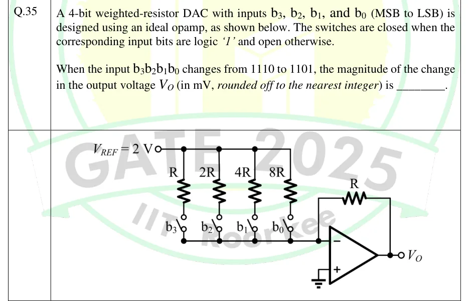
A 4-bit weighted-resistor DAC with inputs , , , and (MSB to LSB) is designed using an ideal opamp, as shown below. The switches are closed when the corresponding input bits are logic '1' and open otherwise.
When the input changes from 1110 to 1101, the magnitude of the change in the output voltage (in mV, rounded off to the nearest integer) is ________.
 Tap to open full size
A reference source V_REF = 2 V drives a common top rail. Four resistors hang from this rail in parallel, from left to right: R, 2R, 4R, 8R. Each resistor's lower end goes through a single-pole switch labelled, left to right, b_3, b_2, b_1, b_0 (so b_3 is in series with R, b_2 with 2R, b_1 with 4R, b_0 with 8R). The far sides of all four switches join a common bottom node, which connects to the inverting (−) input of an ideal op-amp. A feedback resistor R runs from the op-amp output back to the inverting input. The non-inverting (+) input is grounded. The output is labelled V_O.
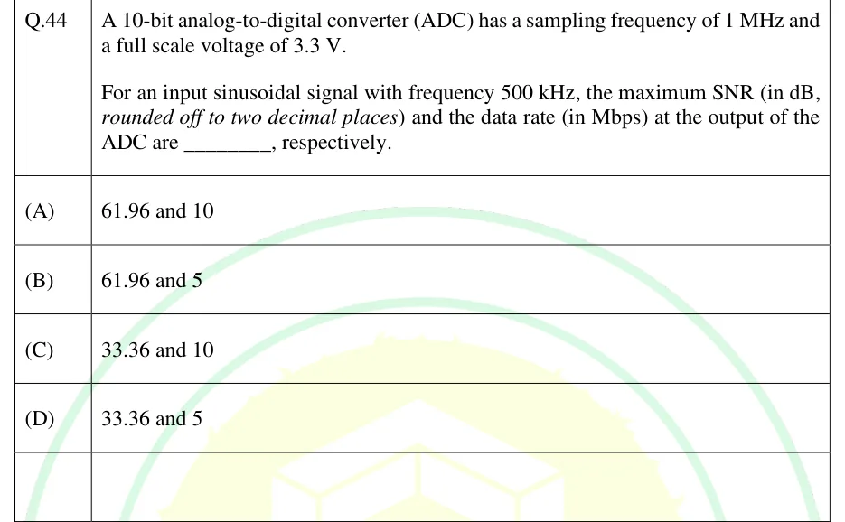
A 10-bit analog-to-digital converter (ADC) has a sampling frequency of 1 MHz and a full scale voltage of 3.3 V.
For an input sinusoidal signal with frequency 500 kHz, the maximum SNR (in dB, rounded off to two decimal places) and the data rate (in Mbps) at the output of the ADC are ________, respectively.
61.96 and 10
61.96 and 5
33.36 and 10
33.36 and 5
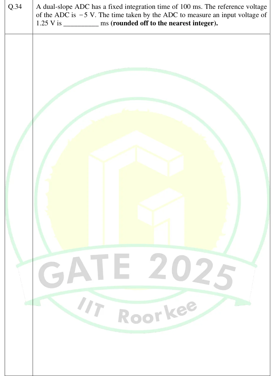
A dual-slope ADC has a fixed integration time of 100 ms. The reference voltage of the ADC is . The time taken by the ADC to measure an input voltage of is __________ ms (rounded off to the nearest integer).
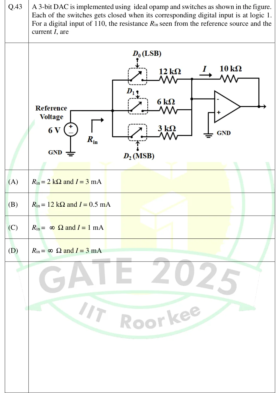
A 3-bit DAC is implemented using ideal opamp and switches as shown in the figure. Each of the switches gets closed when its corresponding digital input is at logic 1. For a digital input of 110, the resistance seen from the reference source and the current , are
 Tap to open full size
Binary-weighted-resistor DAC with an inverting op-amp summer. A 6 V reference voltage source (+ terminal up, − terminal to GND) drives a vertical bus; an arrow labelled R_in points into the bus from the source side. Three single-pole switches (dashed boxes), each on its own branch, have one terminal on this bus. Top branch: switch controlled by D_0 (LSB) in series with 12 kΩ. Middle branch: switch controlled by D_1 in series with 6 kΩ. Bottom branch: switch controlled by D_2 (MSB) in series with 3 kΩ. The far ends of the three resistors join on a second vertical bus. That bus goes to the inverting (−) input of the op-amp. From the top node of the bus, a current I (arrow pointing right) flows through a 10 kΩ feedback resistor to the op-amp output. The non-inverting (+) input is connected to GND. An open switch leaves its resistor disconnected (floating); it is not switched to ground.
and
and
and
and
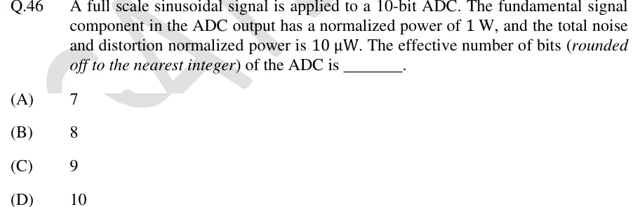
A full scale sinusoidal signal is applied to a 10-bit ADC. The fundamental signal component in the ADC output has a normalized power of 1 W, and the total noise and distortion normalized power is 10 W. The effective number of bits (rounded off to the nearest integer) of the ADC is ________.
7
8
9
10
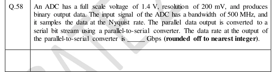
An ADC has a full scale voltage of 1.4 V, resolution of 200 mV, and produces binary output data. The input signal of the ADC has a bandwidth of 500 MHz, and it samples the data at the Nyquist rate. The parallel data output is converted to a serial bit stream using a parallel-to-serial converter. The data rate at the output of the parallel-to-serial converter is ______ Gbps (rounded off to nearest integer).
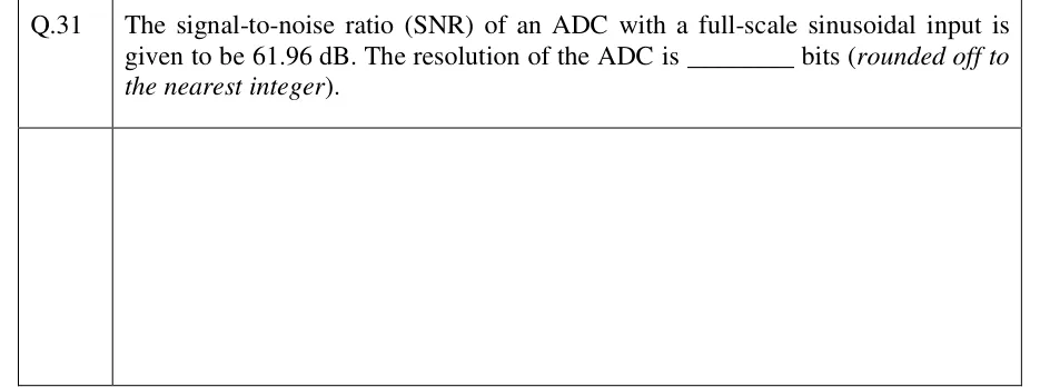
The signal-to-noise ratio (SNR) of an ADC with a full-scale sinusoidal input is given to be 61.96 dB. The resolution of the ADC is ________ bits (rounded off to the nearest integer).
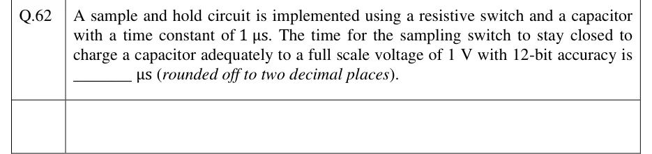
A sample and hold circuit is implemented using a resistive switch and a capacitor with a time constant of 1 μs. The time for the sampling switch to stay closed to charge a capacitor adequately to a full scale voltage of 1 V with 12-bit accuracy is ________ μs (rounded off to two decimal places).
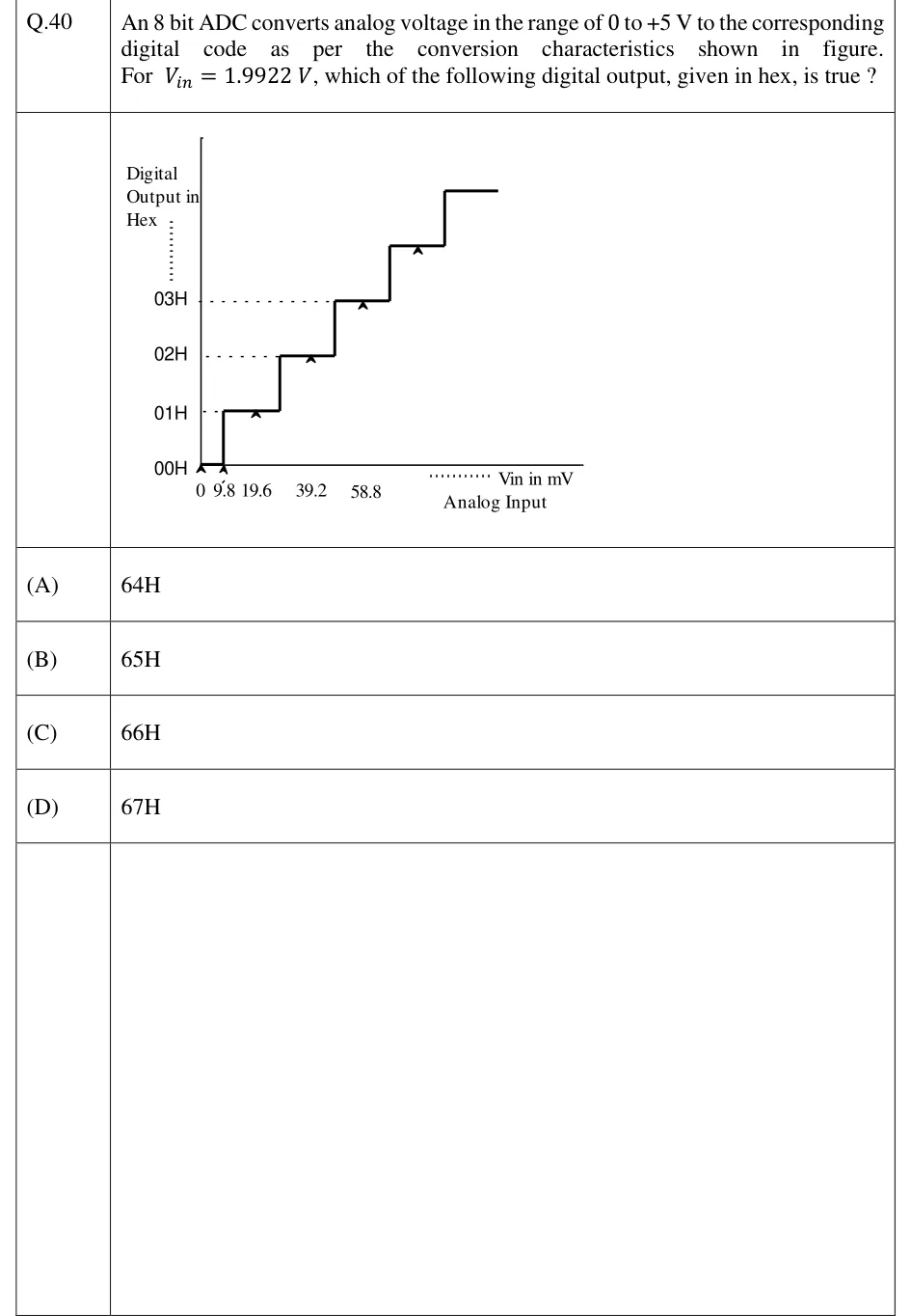
An 8 bit ADC converts analog voltage in the range of 0 to +5 V to the corresponding digital code as per the conversion characteristics shown in figure. For , which of the following digital output, given in hex, is true?
 Tap to open full size
The ADC transfer characteristic, drawn as a staircase. The vertical axis is labelled "Digital Output in Hex" and has ticks 00H, 01H, 02H and 03H, with a dotted line continuing above. The horizontal axis is labelled "Vin in mV / Analog Input" and has tick labels 0, 9.8, 19.6, 39.2 and 58.8, with a dotted line continuing to the right. The staircase stays at 00H from 0 to 9.8 mV and steps up to 01H at 9.8 mV. It steps up to 02H halfway between 19.6 and 39.2 (about 29.4 mV) and to 03H halfway between 39.2 and 58.8 (about 49 mV). Two more unlabelled steps (04H, 05H) follow, then a flat top. Small upward arrowheads mark the middle of each tread: 01H at 19.6 mV, 02H at 39.2 mV, 03H at 58.8 mV, the next step at about 78.4 mV. Two more arrowheads sit on the axis at 0 and 9.8 mV. Dashed horizontal lines join the 01H, 02H and 03H ticks to their treads. So every code k is centred on k × 19.6 mV, and code changes happen at (k - 1/2) × 19.6 mV.
64H
65H
66H
67H
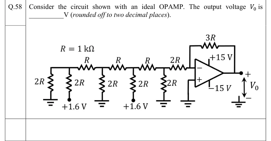
Consider the circuit shown with an ideal OPAMP. The output voltage is ________ V (rounded off to two decimal places).
 Tap to open full size
An R-2R resistor ladder drives an inverting op-amp amplifier, with R = 1 k Ω. The top rail of the ladder, from left to right: node A, then a series R to node B, a series R to node C, a series R to node D, and a series 2R to the inverting (−) input of the op-amp. Shunt resistors: node A has two, a 2R to ground (the leftmost resistor) and a 2R to a +1.6 V source. Node B has a 2R to ground. Node C has a 2R to a +1.6 V source. Node D has a 2R to ground. The non-inverting (+) input is grounded. A feedback resistor 3R connects the output to the inverting input. The supply rails are +15 V and -15 V. The output V_0 is measured from the output terminal (+) to ground (−).
An analog-to-digital converter with resolution 0.01 V converts analog signals between 0 V to +10 V to an unsigned binary output. The minimum number of bits (in integer) in the output is ________
A 10-bit D/A converter is calibrated over the full range from 0 to 10 V. If the input to the D/A converter is 13A (in hex), the output (rounded off to three decimal places) is ________ V.
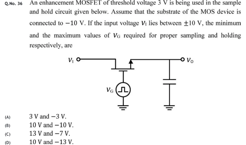
An enhancement MOSFET of threshold voltage 3 V is being used in the sample and hold circuit given below. Assume that the substrate of the MOS device is connected to V. If the input voltage lies between V, the minimum and the maximum values of required for proper sampling and holding respectively, are
 Tap to open full size
Sample-and-hold circuit. The input terminal V_I is wired to the left channel terminal of an enhancement MOSFET. The MOSFET is drawn upside down: the channel line is horizontal at the top and the gate plate sits just below it. The right channel terminal is wired to the output terminal V_O, and that lead carries an arrow pointing away from the channel (upward). This is the simplified n-channel symbol with the arrow on the source lead. No separate substrate terminal is drawn. A capacitor runs from the V_O node to ground. The gate is driven by a pulse voltage source labelled V_G (a circle containing a single rectangular pulse), and the other end of that source is grounded. The question text says the substrate is connected to -10 V.
3 V and V.
10 V and V.
13 V and V.
10 V and V.
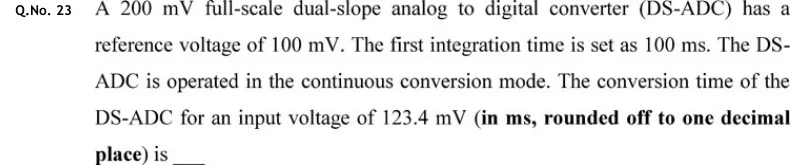
A 200 mV full-scale dual-slope analog to digital converter (DS-ADC) has a reference voltage of 100 mV. The first integration time is set as 100 ms. The DS-ADC is operated in the continuous conversion mode. The conversion time of the DS-ADC for an input voltage of 123.4 mV (in ms, rounded off to one decimal place) is ____
The address lines of a 10 bit, 1.023 V full-scale digital to analog converter (DAC) is connected to the data lines to of an 8-bit microprocessor, with and of the DAC grounded. Now, is changed from 1010 1010 to 1010 1011. The corresponding change in the output of the DAC (in mV, rounded off to one decimal place) is ____
The number of comparators required for implementing an 8-bit flash analog-to-digital converter is
8
128
255
256
PRACTICE
A 10-bit counter-type (digital-ramp) ADC and a 10-bit successive-approximation ADC run from the same clock. The counter-type ADC resets to zero at the start of every conversion and needs clock periods in the worst case. The SAR ADC needs clock periods. The ratio of the worst-case conversion time of the counter-type ADC to that of the SAR ADC is
10.23
102.3
102.4
1023
Answer: (B)
Counter-type worst case: .
SAR: .
Ratio . Option C (102.4) comes from wrongly using .
A sample-and-hold feeds a 12-bit ADC with V (step ). The S/H stays in hold for the ADC's whole conversion time of s, and the total leakage current at the hold capacitor is 10 nA. The minimum hold capacitance (in pF) that keeps the droop during a conversion within LSB is ______.
Answer: (accepted range )
mV, so LSB mV.
The droop requirement mV gives .
F pF.
An ideal 8-bit DAC (straight binary, zero offset, linear) gives an output of 5.10 V for the input 11111111. Its output (in volts) for the input 10000000 is ______.
Answer: (accepted range )
The given value is the full-scale output, i.e. the output for the all-ones code , so V.
The input 10000000 is , so V.
Dividing by instead would wrongly give mV and V.
A 4-bit weighted-resistor DAC uses an ideal inverting op-amp summer with feedback resistor k. The bit resistors are 10 k (MSB ), 20 k (), 40 k () and 80 k (LSB ). A bit equal to 1 connects its resistor to V, and a bit equal to 0 connects it to ground. For the input , the output voltage (in volts, with sign) is ______.
Answer: (accepted range )
Currents into the virtual ground: gives mA; gives 0; gives mA; gives mA.
Total current mA.
V. Formula check: V.
An 8-bit SAR ADC has V, so its internal DAC gives mV for code (MSB first). At each trial the bit is kept if and cleared otherwise. For a held input V, the final output code is
10011110
10011111
10100000
10011100
Answer: (A)
Trials: V, keep; V, clear; V, clear; V, keep.
V, keep; V, keep; V, keep; V V, clear.
Final code . Check: . Option B (159) is what a rounding converter would give, not this truncating SAR.
Which of the following statements is/are correct?
In a dual-slope integrating ADC, the output count does not depend on the integrator's and or on the clock frequency, provided these stay constant during a conversion.
A 6-bit flash ADC needs 64 comparators.
An ADC with a measured SINAD of 50 dB for a full-scale sine has an effective number of bits of about 8.
In a first-order sigma-delta ADC with , doubling the oversampling ratio raises the in-band SQNR by about 9 dB.
Answer: (A), (C), (D)
A: correct. gives . cancels, and the clock cancels because both times are counted with it.
B: wrong. A 6-bit flash needs comparators.
C: correct. .
D: correct. With first-order noise shaping and , in-band SQNR rises as , i.e. dB per doubling.
OFFICIAL GATE 2027 SYLLABUS WORDING
Copied from the GATE 2027 syllabus; see all 2027 syllabi.
GATE EC
Data Converters: Sample and hold circuits, ADCs and DACs
GATE EE
sample and hold circuits, A/D and D/A converters
GATE IN
Analog front end: analog multiplexer, programmable gain amplifier, sample-and-hold circuit; analog-to-digital converters (ADC) (successive approximation, integrating, flash and sigma-delta) and digital-to-analog converters (DAC) (weighted R, R-2R ladder and current steering logic); characteristics and specifications of ADC and DAC
Preparing in Kolkata? IAE Academy's course for GATE ECE, GATE EE or GATE IN.