
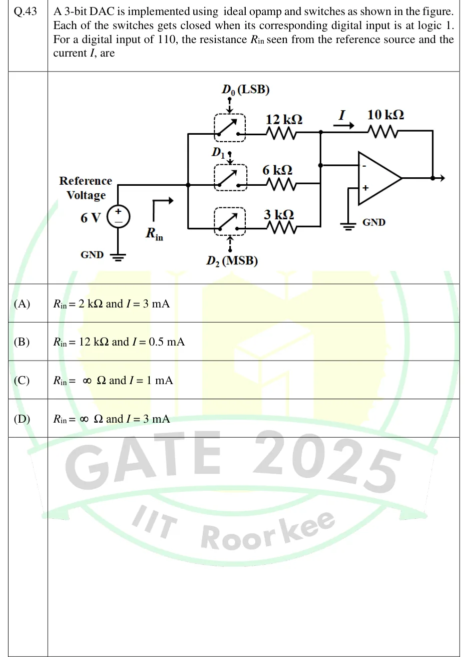
A 3-bit DAC is implemented using ideal opamp and switches as shown in the figure. Each of the switches gets closed when its corresponding digital input is at logic 1. For a digital input of 110, the resistance seen from the reference source and the current , are
 Tap to open full size
Figure description
Binary-weighted-resistor DAC with an inverting op-amp summer. A 6 V reference voltage source (+ terminal up, − terminal to GND) drives a vertical bus; an arrow labelled R_in points into the bus from the source side. Three single-pole switches (dashed boxes), each on its own branch, have one terminal on this bus. Top branch: switch controlled by D_0 (LSB) in series with 12 kΩ. Middle branch: switch controlled by D_1 in series with 6 kΩ. Bottom branch: switch controlled by D_2 (MSB) in series with 3 kΩ. The far ends of the three resistors join on a second vertical bus. That bus goes to the inverting (−) input of the op-amp. From the top node of the bus, a current I (arrow pointing right) flows through a 10 kΩ feedback resistor to the op-amp output. The non-inverting (+) input is connected to GND. An open switch leaves its resistor disconnected (floating); it is not switched to ground.
- (A)
and
- (B)
and
- (C)
and
- (D)
and