
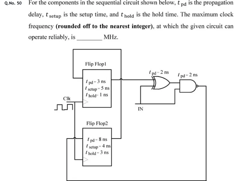
For the components in the sequential circuit shown below, is the propagation delay, is the setup time, and is the hold time. The maximum clock frequency (rounded off to the nearest integer), at which the given circuit can operate reliably, is ________ MHz.
 Tap to open full size
Figure description
Two positive-edge-triggered flip-flops share one clock (Clk, drawn as a square wave on the left, wired to the clock input (triangle) of both). Flip Flop1 is labelled t_pd = 3 ns, t_setup = 5 ns, t_hold = 1 ns. Flip Flop2 is labelled t_pd = 8 ns, t_setup = 4 ns, t_hold = 3 ns. Flip Flop1's output (right side) runs right to one input of a 2-input XOR gate (t_pd = 2 ns). The XOR's second input comes from an external line marked IN, and IN also feeds the second input of a 2-input NAND gate (t_pd = 2 ns). The XOR output goes to the NAND's first input. The NAND output runs right, down along the bottom of the drawing, back left and up into the D input (left side) of Flip Flop2. Flip Flop2's output (right side) runs right to a vertical wire. That wire goes up, crosses Flip Flop1's output line at a hop (no connection), continues over the top of Flip Flop1 and comes down into Flip Flop1's D input (left side). So the two register-to-register paths are FF1 -> XOR -> NAND -> FF2 and FF2 -> FF1 directly.