
IAE Academy

GATE 2023 EC Q.34: solution and answer

GATE 2023 · ECQ.34 · 1 mark · NAT

For the circuit shown below, the propagation delay of each NAND gate is 1 ns. The critical path delay, in ns, is ________ (rounded off to the nearest integer).
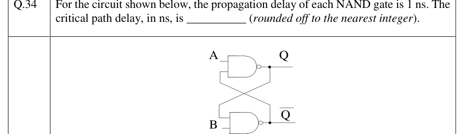
GATE 2023 EC question 34: Two cross-coupled 2-input NAND gates (a NAND SR latch).Tap to open full size
Figure from the GATE 2023 EC paper. It is part of the question.
Figure description

Two cross-coupled 2-input NAND gates (a NAND SR latch). Top NAND gate: upper input is external input A; lower input is fed back from the output of the bottom NAND gate. Its output is labelled Q (a dot marks the junction where Q is tapped for feedback). Bottom NAND gate: upper input is fed back from the Q output of the top gate; lower input is external input B. Its output is labelled Q (with a junction dot where it is tapped for feedback). The two feedback wires cross each other in an X between the gates. No clock is present.

Answer and solution

ANSWER

The critical path delay is 2 ns. An input change goes through its own NAND gate (1 ns), then through the cross-coupled NAND gate (1 ns), and after that both outputs are stable.

Official answer: 02Source: Official answer key, GATE 2023 EC (IIT Kanpur)

  1. Identify the circuit. The two cross-coupled NAND gates form an latch with active-low inputs. sets it () and resets it (). An overline marks the complement, e.g. .

  2. Critical path means the longest input-to-output path before both outputs settle. A change on an input passes through its own gate to change that gate's output. The new output then travels along the feedback wire into the other gate, which changes the second output.

  3. Trace a set operation. Start from the stored state with . This state is consistent: the top NAND sees and gives , and the bottom NAND sees and gives . Now let go . The top NAND has a 0 on an input, so after .

  4. The second gate responds. The bottom NAND now sees and , so after another .

  5. The feedback closes the loop with no further change. goes back into the top NAND, which already has , so stays at 1. Nothing else switches and the latch is stable. Resetting through is the same by symmetry.

  6. Critical path delay.

KEY IDEA

In a cross-coupled NAND (SR) latch, the worst case is an input change that switches its own gate and then, through the feedback wire, switches the other gate. That makes two gate delays. Once the second output reaches the first gate, it only confirms the value already there, so the loop does not keep going round.

WATCH OUT FOR

Answering 1 ns, which counts only the gate the input drives and ignores that settles one gate delay later. The opposite mistake is thinking the feedback loop adds delays without end (or a third delay). The feedback signal arrives at the first gate without changing its output, so the circuit is settled after 2 ns.

From the GATE 2023 EC paper. Every question of this paper · Download the full paper · All 30 Sequential questions, with notes

More Sequential questions