
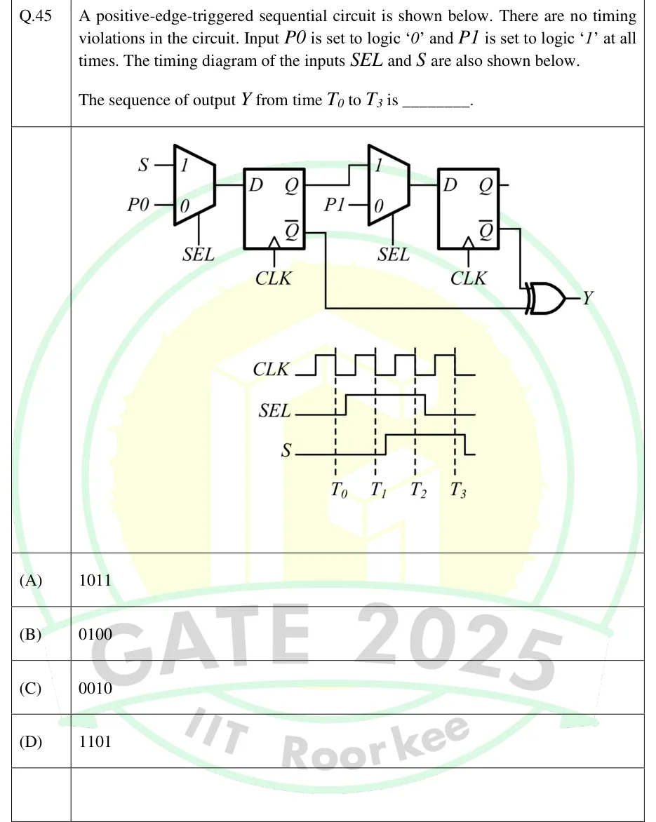
A positive-edge-triggered sequential circuit is shown below. There are no timing violations in the circuit. Input is set to logic '0' and is set to logic '1' at all times. The timing diagram of the inputs and are also shown below.
The sequence of output from time to is ________.
 Tap to open full size
Figure description
Circuit: a 2:1 MUX (MUX1) has input 1 = S, input 0 = P0 and select line SEL. Its output drives the D input of D flip-flop FF1, which is positive-edge triggered on CLK. The Q output of FF1 goes to input 1 of a second 2:1 MUX (MUX2). Input 0 of MUX2 is P1, and its select line is SEL. The MUX2 output drives the D input of D flip-flop FF2, also positive-edge triggered on CLK. FF2's Q output is an unconnected stub. A 2-input XOR gate has output Y. One XOR input is the Q-bar output of FF2. The other XOR input is the Q-bar output of FF1, routed down and along beneath the circuit. Timing diagram: CLK starts low and has four pulses. Vertical dashed lines labelled T0, T1, T2 and T3 fall on the four falling edges of CLK, so each rising edge lies between the previous dashed line and the next. SEL is 0 until just after T0 (before the next rising edge), then 1 until just after T2 (again before the next rising edge), then 0. S is 0 until just after T1 (before the next rising edge), then 1 until just after T3, then 0.
- (A)
1011
- (B)
0100
- (C)
0010
- (D)
1101