GATE 2026 EE Q.48
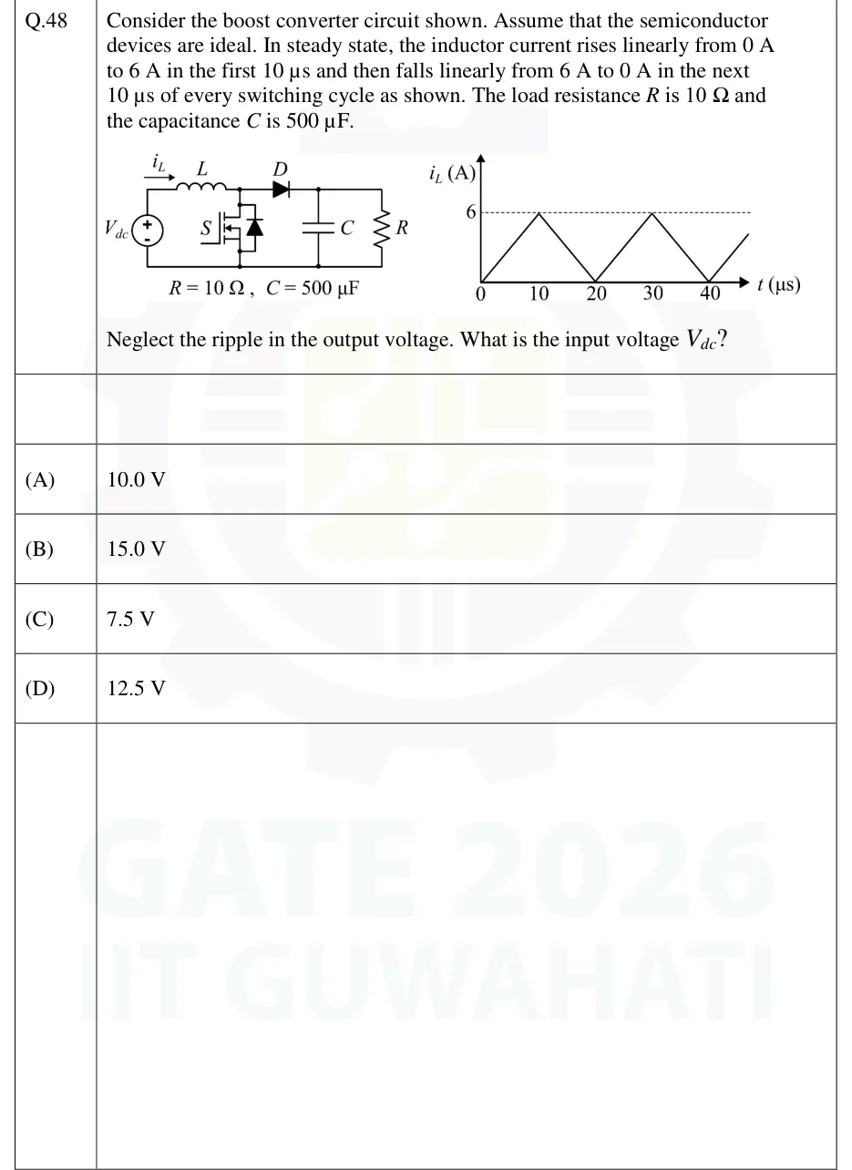
Consider the boost converter circuit shown. Assume that the semiconductor devices are ideal. In steady state, the inductor current rises linearly from 0 A to 6 A in the first 10 µs and then falls linearly from 6 A to 0 A in the next 10 µs of every switching cycle as shown. The load resistance R is 10 Ω and the capacitance C is 500 µF. Neglect the ripple in the output voltage. What is the input voltage V_dc?
 Tap to open full size
Figure description
Left: boost converter. Source V_dc (+ at top) in series with inductor L (current i_L flowing left to right) to the switch-diode node. MOSFET S (with its body diode) connects from that node to the bottom rail. Diode D goes from that node to the output node (anode at the node), then capacitor C and load R in parallel from the output node to the bottom rail. Labelled R = 10 Ω, C = 500 µF. Right: plot of i_L (A) versus t (µs): a triangular waveform from 0 at t = 0 rising to 6 A at 10 µs (dashed line marks 6), falling to 0 at 20 µs, rising to 6 A at 30 µs, falling to 0 at 40 µs, and so on. The time axis is marked 0, 10, 20, 30, 40.
- (A)
10.0 V
- (B)
15.0 V
- (C)
7.5 V
- (D)
12.5 V