IAE Academy

IN THE EE SYLLABUS

Power semiconductor switches and their gating

This topic covers the static V-I characteristics of the thyristor (SCR), power MOSFET and IGBT, with the power diode, TRIAC and GTO for comparison, and how each device is switched on and off by its gate. Typical problems involve latching and holding current, R and UJT triggering, gate pulse width, commutation time, di/dt and dv/dt limits, and loss and gate-charge arithmetic. Knowing which device is current-triggered or voltage-controlled, and what turns each one off, settles many conceptual questions quickly.

9 previous-year questions · 9 solved · 6 practice questions

Power diode and the thyristor: structure and static V-I characteristic

A power diode is a - junction with a lightly doped, thick drift region () that lets it block high reverse voltage. It conducts when forward biased and blocks when reverse biased. When it is switched off, its stored charge must first be removed, so a reverse current flows for the reverse recovery time before the diode regains its blocking ability.

The thyristor (SCR) is a four-layer --- device with three junctions () and three terminals: anode (A), cathode (K) and gate (G). It is a latching, current-triggered device. It can be turned on by a gate pulse but, in a conventional SCR, cannot be turned off by the gate.

Regions of the static V-I characteristic

  1. Reverse blocking: A negative with respect to K. and are reverse biased and only a small leakage current flows, until reverse breakdown.

  2. Forward blocking (OFF state): A positive, no gate current. is reverse biased and only a small leakage current flows.

  3. Forward breakover: if reaches the forward breakover voltage , the device switches to the ON state without any gate signal. falls as the gate current rises.

  4. Forward conduction (ON state): the drop is small (typically about 1 to 2 V). The device stays on as long as the anode current stays above the holding current.

TWO-TRANSISTOR MODEL OF THE SCR

The SCR is modelled as a -- transistor (common-base current gain ) and an -- transistor (gain ), with the gate current feeding the base of ; and are their leakage currents. The gains rise with current. As the anode current is limited only by the external circuit: the device has latched.

LATCHING AND HOLDING CURRENT

Latching current is the minimum anode current that must be reached before the gate pulse is removed for the SCR to stay on. Holding current is the anode current below which a conducting SCR (gate open) turns off. Typically is about two to three times .

THYRISTOR CONDUCTION (AVERAGE) LOSS

Piecewise-linear on-state model : threshold voltage and dynamic resistance , with the average and rms values of the SCR current taken over a full period.

Turn-on methods, gate characteristics and triggering circuits

Ways to turn an SCR on

  1. Gate current (the normal, controlled method).

  2. Forward-voltage breakover (): not used for control, and it can damage the device.

  3. dv/dt turn-on: a fast-rising forward voltage drives a charging current through the capacitance of the reverse-biased junction , which can trigger the device falsely.

  4. Temperature: leakage current grows with temperature and can turn the device on.

  5. Light (light-activated SCR).

DV/DT (FALSE) TRIGGERING CURRENT

Charging current of the junction capacitance of ( taken as constant). If this current reaches the triggering level, the SCR turns on with no gate signal; this sets the device's critical rating.

The gate characteristic is the plot of against for the gate-cathode junction; devices of one type spread between a minimum and a maximum curve. Reliable triggering needs the operating point to lie inside the preferred firing area, bounded below by the minimum gate voltage and current that trigger every device of the type, and above by the maximum gate voltage, current and power (). The trigger source with source resistance gives a load line.

GATE LOAD LINE AND SERIES RESISTOR

is the open-circuit trigger source voltage; the operating point is where this line meets the gate characteristic.

PULSE GATING: PEAK AND AVERAGE GATE POWER

For a rectangular gate pulse train of width at frequency , the average gate power is . A short pulse may therefore carry a peak power above the average gate power rating , as long as it stays within the device's peak gate power limit.

The gate pulse must last long enough for the anode current to rise above . With an inductive load the anode current rises slowly, so a wide pulse or a train of pulses is needed. Isolation between the gate circuit and the power circuit is normally provided by a pulse transformer or an optocoupler.

MINIMUM GATE PULSE WIDTH WITH AN R-L LOAD

A dc supply is switched by the SCR onto a series - load, with the current starting from zero. The current must reach before the gate pulse ends. The approximation holds when .

R TRIGGERING (HALF-WAVE, AC SUPPLY)

Supply ; is measured from the positive-going zero crossing of the supply. The SCR fires when the supply reaches the value that drives through the total series gate-circuit resistance (including the minimum fixed resistor) with across the gate junction (the series diode drop neglected). Since a sine peaks at , the range is about to . Increasing delays firing.

RC triggering adds a capacitor whose voltage lags the supply, so the firing angle can be delayed well beyond , approaching (but in practice short of) , by increasing or .

UJT RELAXATION OSCILLATOR

is the intrinsic stand-off ratio. charges through from until reaches the peak-point voltage ; the UJT then fires and discharges quickly through (or a pulse transformer), giving a gate pulse. This form neglects , the valley voltage and the discharge time.

UJT OSCILLATOR: EXACT CHARGING TIME AND THE RANGE OF R

Here the capacitor discharges only down to the valley voltage , and keeps the diode drop . and are the peak-point and valley-point currents. The upper limit on lets enough current reach the emitter to fire the UJT; the lower limit lets it turn off again so that the circuit oscillates. With and this reduces to the simple form above.

EXAM TIP

In the simple form, the UJT oscillator frequency depends on , and only, not on (the supply cancels in the ratio when is small). To lock the gate pulses to the ac supply, is taken from a zener-clipped rectified supply: it falls to zero at each supply zero crossing, which resets the capacitor.

Turn-off, commutation, di/dt and dv/dt protection

An SCR turns off when its anode current falls below and it is then held reverse biased long enough for the stored carriers near to recombine. The minimum such time is the device turn-off time (reverse recovery time plus gate recovery time). Forward voltage must not be reapplied before then: the circuit turn-off time must satisfy , otherwise the SCR turns on again.

Type

How the anode current is brought to zero

Where it is used

Natural (line) commutation

The ac supply voltage itself reverses

Phase-controlled rectifiers, ac voltage controllers

Forced commutation

An added circuit (charged capacitor, LC) reverse biases the SCR

DC choppers and inverters fed from dc

Load commutation

The load (a leading power factor or underdamped resonant load) brings the SCR current to zero and leaves a reverse voltage across it

Load-commutated and resonant inverters

CAPACITOR COMMUTATION TIME

A dc supply feeds a purely resistive load through the SCR. A capacitor charged to in the reverse-biasing polarity is connected directly across the conducting SCR (auxiliary switch drop neglected). The SCR turns off and recharges through , so the SCR voltage is . It passes through zero at this time, which is how long the SCR is held reverse biased.

RESONANT (SELF) COMMUTATION, SERIES R-L-C

A series -- circuit is switched onto a dc supply by the SCR, with uncharged and no initial current, and underdamped (). The current falls to zero by itself at and the SCR turns off. By then the capacitor has charged above , so the SCR is left reverse biased.

DI/DT LIMIT WITH SERIES INDUCTOR

At the instant of turn-on the whole supply appears across the series inductor (other resistances neglected), so . Conduction starts near the gate and spreads slowly, so a small inductor in series with the SCR protects it from local hot-spot burn-out.

dv/dt protection uses an RC snubber across the SCR. The capacitor slows the rise of the forward voltage. The series resistor limits the capacitor's discharge current into the SCR at turn-on; the peak discharge current is about . It also damps the oscillation with any series inductance.

EXAM TIP

Do not confuse the two protections: inductor in series = di/dt, RC across the device = dv/dt.

TRIAC and GTO in brief

A TRIAC behaves like two SCRs in anti-parallel with a single gate. It conducts in both directions and can be triggered by a gate current of either polarity, so it is used for ac phase control. The four trigger modes are named by the sign of MT2 relative to MT1 and the sign of the gate current (gate relative to MT1): I+, I−, III+, III−. I+ and III− are usually the most sensitive, and III+ the least. Compared with an SCR it has lower dv/dt and di/dt ratings and a longer turn-off time, since both halves share one silicon structure, so it is used mainly at power frequency.

A GTO (gate turn-off thyristor) is latched on by a positive gate pulse like an SCR, but can also be turned off by a large negative gate current pulse. It needs no commutation circuit. Its turn-off gain is low (typically about 3 to 5), so the turn-off gate current is a sizeable fraction of the anode current being interrupted, and its gate drive is demanding.

Device

Turn-on

Turn-off

Conducts

SCR

Gate pulse

Anode current below (commutation)

One direction

TRIAC

Gate pulse, either polarity

Current falls below at the ac zero crossing

Both directions

GTO

Positive gate pulse

Large negative gate pulse

One direction

Power MOSFET and IGBT: structure, characteristics and gate drive

The power MOSFET is a voltage-controlled, majority-carrier device. Its gate is insulated from the channel, so in the steady state it draws negligible gate current. But the gate has input capacitance that must be charged and discharged at each switching. With no minority-carrier storage it switches very fast. It has an integral body diode between source and drain (for an n-channel device, anode at the source and cathode at the drain).

Power MOSFET static characteristics

  1. Transfer: the drain current is negligible for (cut-off) and rises with above it.

  2. Output ( against for a fixed ): an ohmic (triode) region, where the device acts as a resistance and is used as a closed switch, and a saturation (constant-current) region. A switching device passes through the saturation region only during transitions, because the dissipation there is high.

  3. rises with temperature (positive temperature coefficient), which helps parallel devices share current and resists thermal runaway.

  4. rises steeply with the voltage rating, so MOSFETs suit lower voltages and high switching frequencies.

The IGBT combines a MOSFET input (voltage-controlled gate) with a bipolar output stage. Conductivity modulation lowers the drift region resistance, which gives a low on-state voltage drop even at high voltage ratings. Its output characteristic ( against for fixed ) shows almost no current until exceeds about one junction drop. It conducts in one direction only and has no integral body diode, so an anti-parallel diode is normally added. Because of minority carriers it turns off more slowly than a MOSFET, with a current tail, which limits its switching frequency. Its four-layer structure contains a parasitic thyristor: if this latches up (excessive collector current), the gate loses control.

Property

Power MOSFET

IGBT

Control

Voltage (gate)

Voltage (gate)

Carriers

Majority only

Majority and minority

On-state drop

, resistive, rises with rating

Roughly a constant plus a resistive part, low even at high rating

Switching speed

Fastest

Slower, current tail at turn-off

Typical use

Low voltage, high frequency

Medium to high voltage and power

GATE DRIVE POWER (MOSFET OR IGBT)

is the total gate charge for the gate voltage swing (from the off level to the on level; equal to when the device is turned off at 0 V), and is the switching frequency. is the power drawn from the driver, and the average current drawn from the driver supply. With a constant gate current , the time to deliver a charge is .

During switching, stays almost constant at the Miller plateau while the gate-drain charge is delivered and swings. With a gate resistance , the gate current during the plateau is about , so the drain-voltage transition takes about .

The safe operating area (SOA) of a MOSFET or IGBT is the region of against in which the device can operate without damage. It is bounded by the maximum current, the maximum voltage and the maximum power dissipation (with a time-dependent allowance for pulses). Gate drive is typically to V to turn on, with zero or a negative voltage to turn off; a negative off-state voltage is common for the IGBT to improve noise immunity.

EXAM TIP

A MOSFET is voltage controlled, but it is not free of gate current while switching: the gate capacitance must be charged. Fast gate drivers matter because the switching time is set by how quickly the gate charge is delivered.

Losses, junction temperature and choosing a device

MOSFET CONDUCTION LOSS

is the rms drain current taken over the whole switching period, and is taken at the operating junction temperature.

IGBT OR DIODE CONDUCTION LOSS

Straight-line model of the on-state drop , with the average and rms values of the device current taken over the whole period.

SWITCHING LOSS, CLAMPED INDUCTIVE SWITCHING

The device switches current against a blocked voltage with an inductive load clamped by a diode. At turn-on the current ramps linearly with the voltage held at , then the voltage falls linearly with the current held at ; turn-off is the reverse. and are the total transition times. The energy per cycle is , and multiplying by gives the power.

SWITCHING LOSS, RESISTIVE LOAD

With a resistive load the voltage and current ramp linearly at the same time, in opposite directions. The energy per transition is .

JUNCTION TEMPERATURE

Steady state. Thermal resistances in C/W: junction-to-case, case-to-sink and sink-to-ambient; is the total device loss.

Need

Natural choice

Very high power, line-frequency, natural commutation

SCR

Very high power with gate turn-off

GTO

ac power control at low power

TRIAC

High frequency, low voltage

Power MOSFET

Medium to high voltage, moderate frequency

IGBT

EXAM TIP

Total loss = conduction + switching (+ gate drive and leakage losses, usually small). Switching loss grows linearly with , so conduction loss usually dominates at low frequency and switching loss at high frequency.

PREVIOUS-YEAR QUESTIONS

9 questions from the EE papers

Try each question first, then open the answer. We placed each question under a topic ourselves; the exam paper does not label topics.

See these papers in full: GATE EE 2026 · GATE EE 2024 · GATE EE 2023 · GATE EE 2022 · GATE EE 2020 · GATE EE 2018

GATE 2026 EE Q.27

GATE 2026 · EEQ.27 · 1 mark · MCQ

The figure shows a straight-line approximation for the forward characteristics of a power diode. A continuous on-state current of 15 A is flowing through the diode. What is the power loss in the diode?
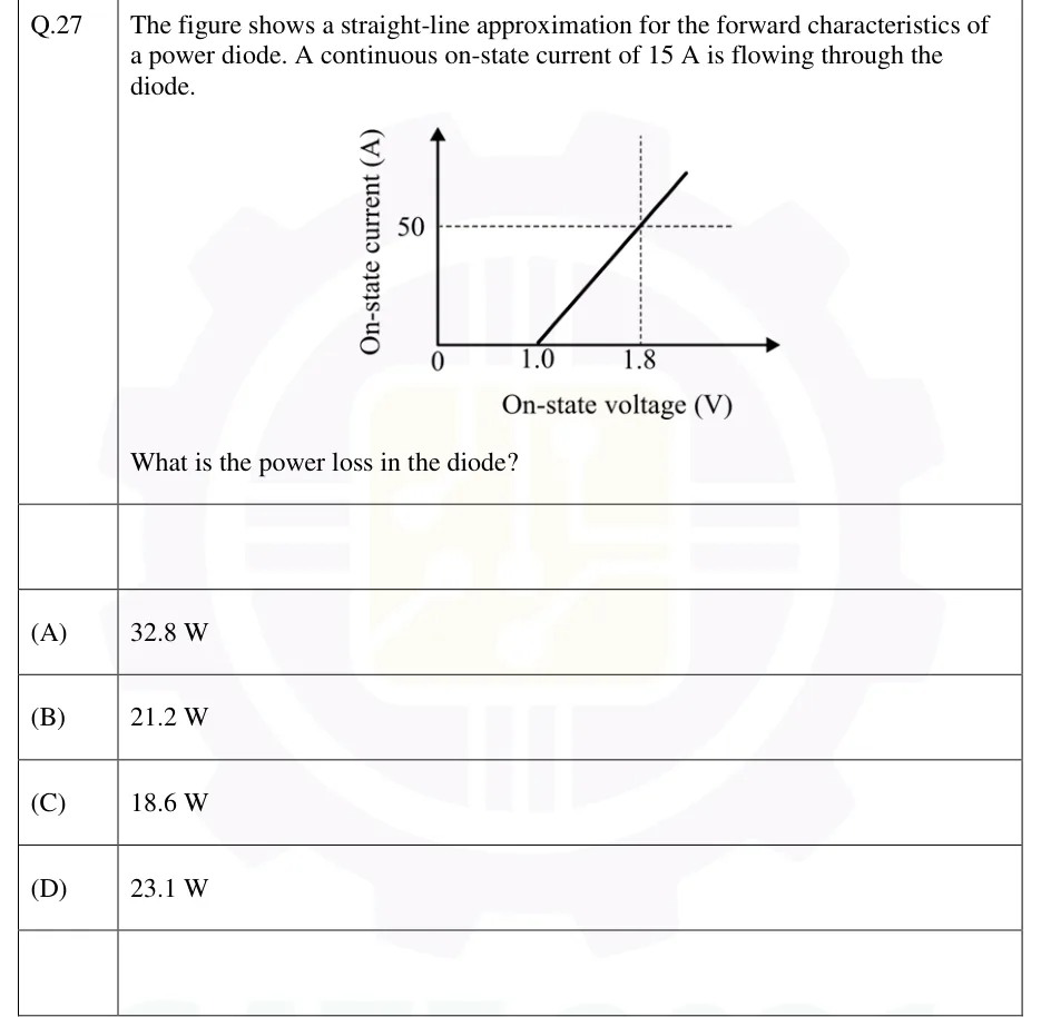
GATE 2026 EE question 27: Plot with horizontal axis 'On-state voltage (V)' and vertical axis 'On-state current (A)', origin 0.Tap to open full size
Figure from the GATE 2026 EE paper. It is part of the question.
Figure description

Plot with horizontal axis 'On-state voltage (V)' and vertical axis 'On-state current (A)', origin 0. A straight line starts on the voltage axis at 1.0 V (zero current) and rises to the right. A dashed horizontal line from the 50 A mark on the current axis and a dashed vertical line from 1.8 V on the voltage axis meet the straight line at the point (1.8 V, 50 A). The line continues slightly beyond that point.

  1. (A)

    32.8 W

  2. (B)

    21.2 W

  3. (C)

    18.6 W

  4. (D)

    23.1 W

Answer and solution
GATE 2026 EE Q.27: answer and solution

GATE 2026 EE Q.28

GATE 2026 · EEQ.28 · 1 mark · MCQ

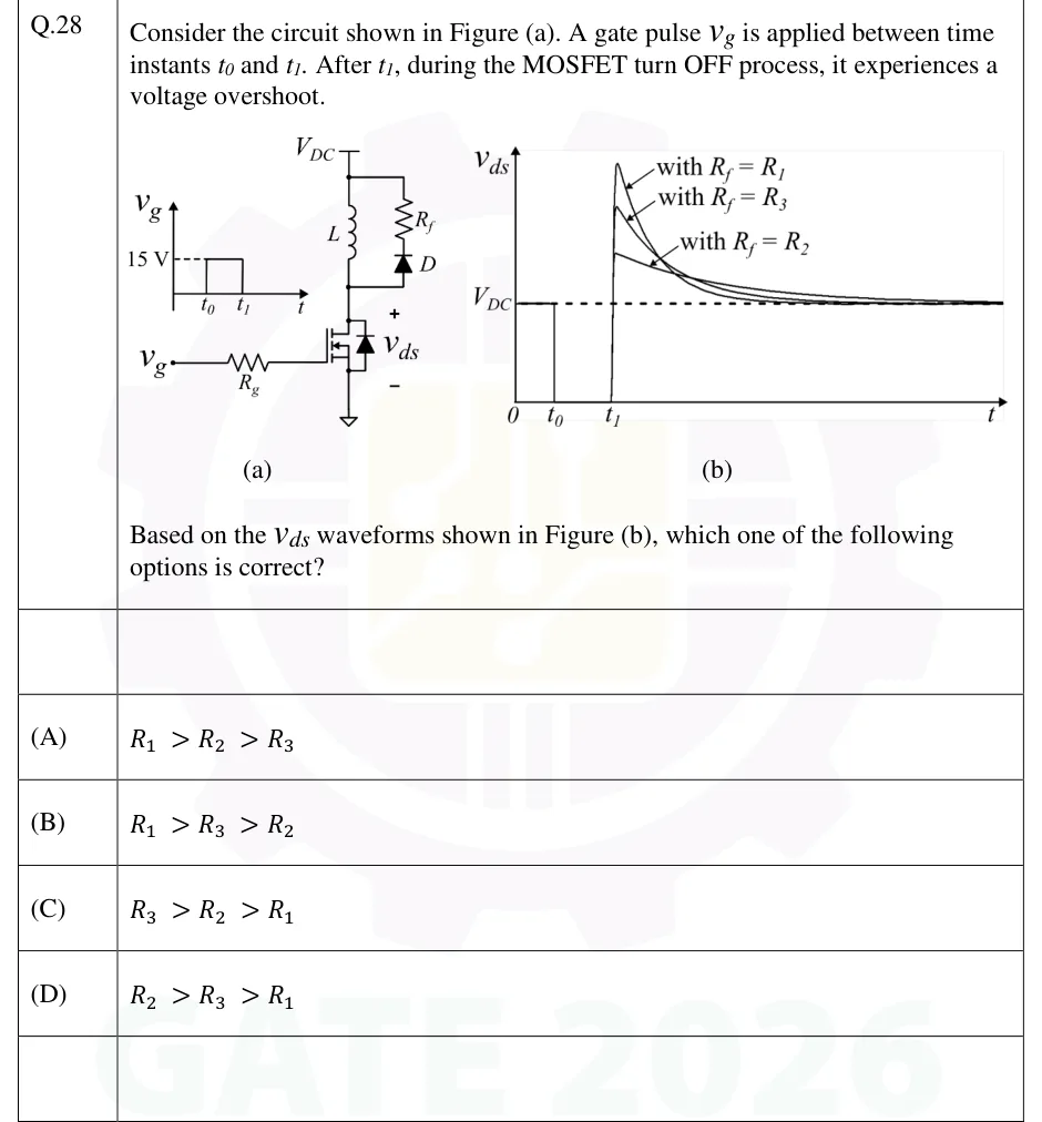
Consider the circuit shown in Figure (a). A gate pulse is applied between time instants and . After , during the MOSFET turn OFF process, it experiences a voltage overshoot. Based on the waveforms shown in Figure (b), which one of the following options is correct?

GATE 2026 EE question 28: Figure (a): a DC supply V_DC feeds, from its top rail, an inductor L in parallel with a series branch of a resistor R_f…Tap to open full size
Figure from the GATE 2026 EE paper. It is part of the question.
Figure description

Figure (a): a DC supply V_DC feeds, from its top rail, an inductor L in parallel with a series branch of a resistor R_f and a diode D. The two branches join at the drain of an n-channel MOSFET whose source is grounded; v_ds is marked + at the drain and - at the source. The R_f-D branch is the freewheeling path for the inductor current (the diode conducts from the drain node up toward the V_DC rail). The gate is driven through R_g from v_g, a rectangular pulse of 15 V between t_0 and t_1. Figure (b): v_ds versus t with a dashed horizontal line at V_DC. v_ds equals V_DC from 0 to t_0, falls to 0 at t_0 (MOSFET ON), stays near 0 until t_1, then at t_1 jumps above V_DC to a peak and decays back to V_DC. Three curves are labelled: with R_f = R_1 has the highest peak and the fastest decay, with R_f = R_3 has a middle peak, with R_f = R_2 has the lowest peak and the slowest decay.

  1. (A)

  2. (B)

  3. (C)

  4. (D)

Answer and solution
GATE 2026 EE Q.28: answer and solution

GATE 2024 EE Q.35

GATE 2024 · EEQ.35 · 1 mark · NAT

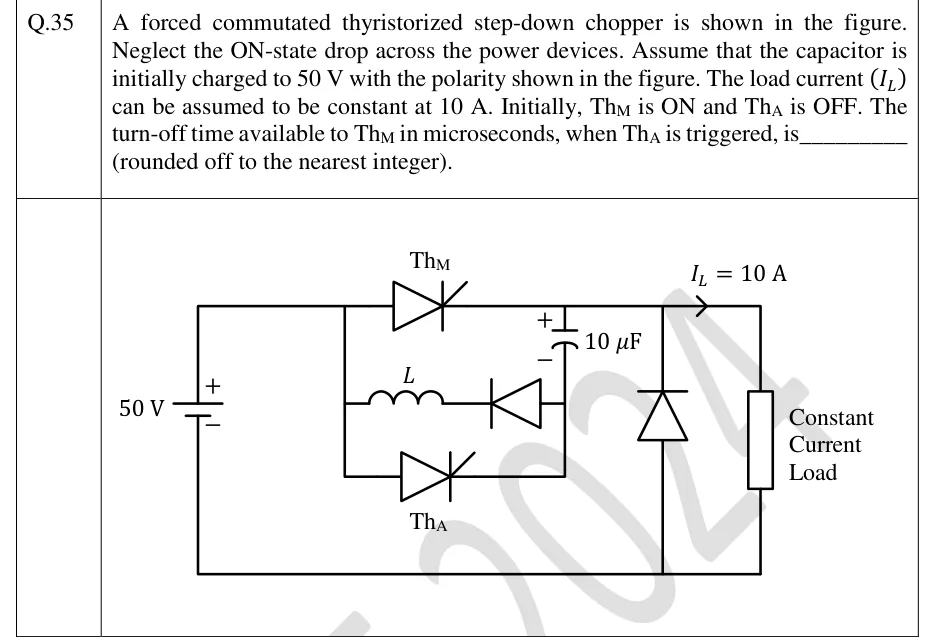
A forced commutated thyristorized step-down chopper is shown in the figure. Neglect the ON-state drop across the power devices. Assume that the capacitor is initially charged to 50 V with the polarity shown in the figure. The load current (I_L) can be assumed to be constant at 10 A. Initially, Th_M is ON and Th_A is OFF. The turn-off time available to Th_M in microseconds, when Th_A is triggered, is ______ (rounded off to the nearest integer).

GATE 2024 EE question 35: A 50 V source (+ on top) feeds the top rail.Tap to open full size
Figure from the GATE 2024 EE paper. It is part of the question.
Figure description

A 50 V source (+ on top) feeds the top rail. Main thyristor Th_M sits in the top branch from the source + rail to the load node. A 10 microfarad capacitor is connected from the load node (+ plate, top) to a junction below (- plate). Middle branch: inductor L in series with a diode, running from the source + rail to the capacitor - plate (diode cathode toward L). Lower branch: auxiliary thyristor Th_A from the source + rail to the capacitor - plate. At the load node a constant-current load I_L = 10 A flows to the bottom rail, with a freewheeling diode across the load (cathode at load node). Bottom rail returns to source -.

Answer and solution
GATE 2024 EE Q.35: answer and solution

GATE 2023 EE Q.26

GATE 2023 · EEQ.26 · 1 mark · MSQ

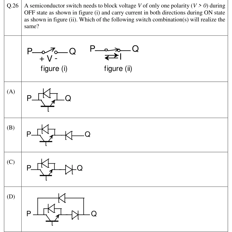
A semiconductor switch needs to block voltage V of only one polarity (V > 0) during OFF state as shown in figure (i) and carry current in both directions during ON state as shown in figure (ii). Which of the following switch combination(s) will realize the same?

GATE 2023 EE question 26: Figure (i): a switch between terminals P (left) and Q (right), open, with voltage V marked + on the P side and - on the Q…Tap to open full size
Figure from the GATE 2023 EE paper. It is part of the question.
Figure description

Figure (i): a switch between terminals P (left) and Q (right), open, with voltage V marked + on the P side and - on the Q side. Figure (ii): the same switch closed, with a double-headed arrow showing current I may flow in both directions between P and Q. Option (A): IGBT with collector at P and emitter at Q, with an antiparallel diode across it (conducting from Q to P). Option (B): the IGBT with antiparallel diode of (A), in series toward Q with a diode that conducts from Q towards P (pointing at the IGBT). Option (C): the IGBT with antiparallel diode of (A), in series toward Q with a diode that conducts from P towards Q. Option (D): the series combination of (C) (IGBT with antiparallel diode, then a diode conducting from P towards Q) with a second diode connected across the whole combination from P to Q, conducting from Q towards P.

  1. (A)

    Figure — IGBT (collector at P, emitter at Q) with an antiparallel diode across it, between P and Q.

  2. (B)

    Figure — IGBT with antiparallel diode, in series with an extra diode that points back towards P (conducts Q to P), between P and Q.

  3. (C)

    Figure — IGBT with antiparallel diode, in series with an extra diode that points towards Q (conducts P to Q), between P and Q.

  4. (D)

    Figure — IGBT with antiparallel diode in series with a diode conducting P to Q, the whole branch connected in parallel with a diode conducting Q to P, between P and Q.

Answer and solution
GATE 2023 EE Q.26: answer and solution

GATE 2023 EE Q.55

GATE 2023 · EEQ.55 · 2 marks · NAT

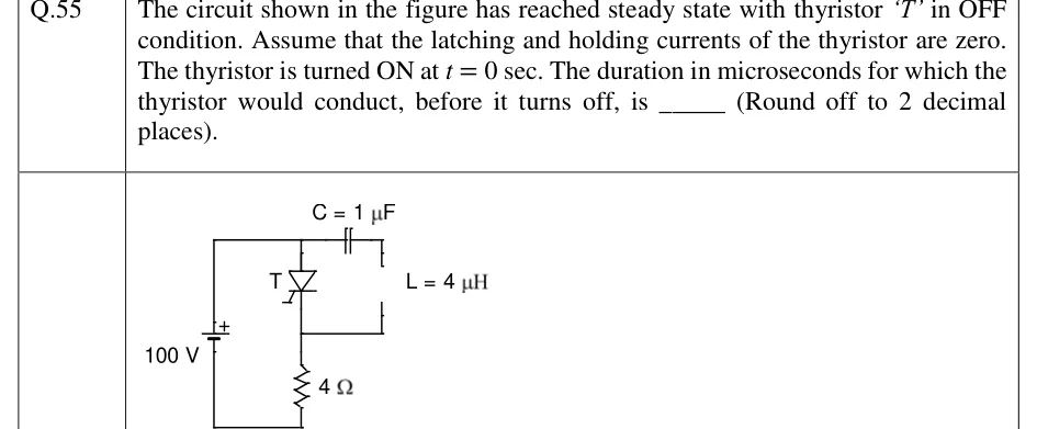
The circuit shown in the figure has reached steady state with thyristor 'T' in OFF condition. Assume that the latching and holding currents of the thyristor are zero. The thyristor is turned ON at t = 0 sec. The duration in microseconds for which the thyristor would conduct, before it turns off, is _____ (Round off to 2 decimal places).

GATE 2023 EE question 55: A 100 V DC source with its + terminal at the top.Tap to open full size
Figure from the GATE 2023 EE paper. It is part of the question.
Figure description

A 100 V DC source with its + terminal at the top. From the + terminal a wire runs up and right to the left plate of a capacitor C = 1 uF. The right plate of C connects through an inductor L = 4 uH to a lower node. A thyristor T sits in the left vertical branch with its anode toward the top wire (+ terminal) and its cathode toward the lower node, so T is in parallel with the series C-L branch. From the lower node a 4 ohm resistor goes down and back to the negative terminal of the source.

Answer and solution
GATE 2023 EE Q.55: answer and solution

GATE 2020 EE Q.20

GATE 2020 · EEQ.20 · 1 mark · NAT

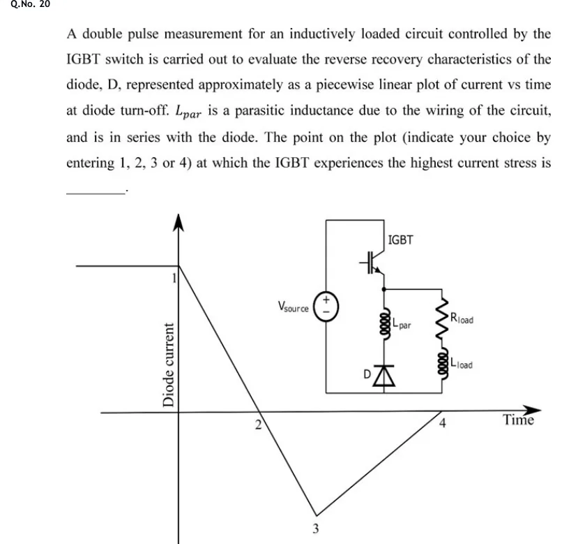
A double pulse measurement for an inductively loaded circuit controlled by the IGBT switch is carried out to evaluate the reverse recovery characteristics of the diode, D, represented approximately as a piecewise linear plot of current vs time at diode turn-off. is a parasitic inductance due to the wiring of the circuit, and is in series with the diode. The point on the plot (indicate your choice by entering 1, 2, 3 or 4) at which the IGBT experiences the highest current stress is ______.

GATE 2020 EE question 20: Left: plot of diode current (vertical axis) versus time (horizontal axis).Tap to open full size
Figure from the GATE 2020 EE paper. It is part of the question.
Figure description

Left: plot of diode current (vertical axis) versus time (horizontal axis). The current is a constant positive level up to time zero (point 1, at the top, where the fall begins). It then falls linearly with a steep slope, crossing zero at point 2, and continues to a negative peak at point 3 (the maximum reverse recovery current). From point 3 it rises linearly back to zero at point 4 on the time axis. Right: circuit with a voltage source V_source (plus at top) feeding an IGBT in series at the top. The IGBT emitter node connects to two parallel branches: the diode branch (L_par in series with diode D, D pointing upward so its anode is at the bottom and its cathode at the top, toward the L_par and IGBT node) and the load branch (R_load in series with L_load). Both branches return to the negative terminal of the source.

Answer and solution
GATE 2020 EE Q.20: answer and solution

GATE 2018 EE Q.4

GATE 2018 · EEQ.4 · 1 mark · MCQ

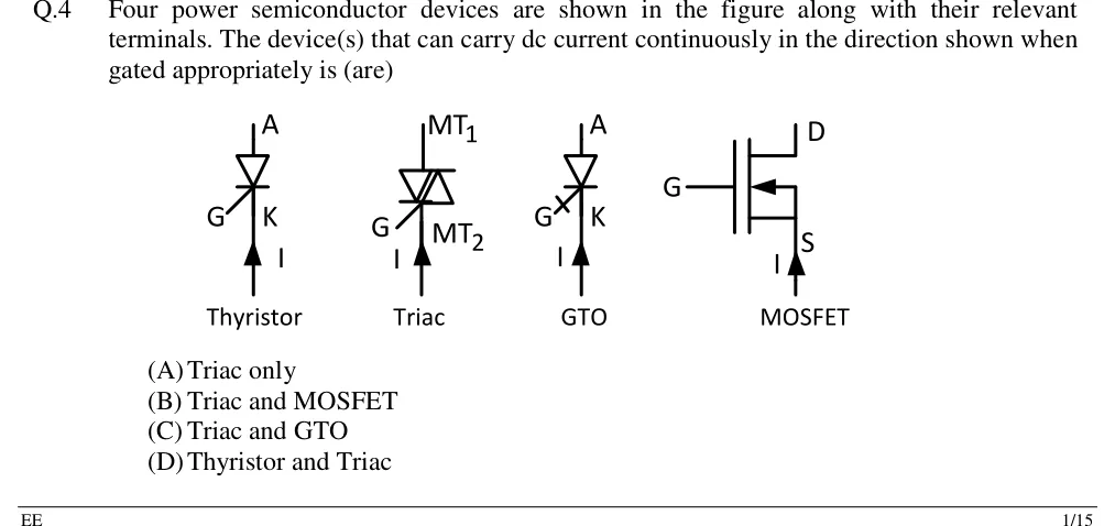
Four power semiconductor devices are shown in the figure along with their relevant terminals. The device(s) that can carry dc current continuously in the direction shown when gated appropriately is (are)

GATE 2018 EE question 4: Four device symbols, each with an upward arrow labelled I drawn at the bottom terminal, showing the current entering the…Tap to open full size
Figure from the GATE 2018 EE paper. It is part of the question.
Figure description

Four device symbols, each with an upward arrow labelled I drawn at the bottom terminal, showing the current entering the lower terminal and flowing upward through the device. (1) Thyristor: anode A at top, cathode K at bottom, gate G on the left side of the cathode end; the arrow I enters at K. (2) Triac: MT1 at top, MT2 at bottom, gate G at lower left; the arrow I enters at MT2. (3) GTO: A at top, K at bottom, gate G at lower left drawn with a cross-bar (GTO symbol); the arrow I enters at K. (4) MOSFET: gate G on the left, drain D at top, source S at bottom; the channel arrow points toward the channel from the source side, so it is an n-channel enhancement MOSFET; the arrow I enters at S, flowing from S to D.

  1. (A)

    Triac only

  2. (B)

    Triac and MOSFET

  3. (C)

    Triac and GTO

  4. (D)

    Thyristor and Triac

Answer and solution
GATE 2018 EE Q.4: answer and solution

PRACTICE

6 questions to test yourself

PRACTICE 12 marks · NAT

A UJT relaxation oscillator uses , and intrinsic stand-off ratio . Neglecting the emitter diode drop, the valley voltage and the discharge time, the oscillation frequency in Hz is ______ (round to the nearest integer).

Answer and solution

Answer: (accepted range )

  1. .

  2. .

  3. Hz, so about 831 Hz.

PRACTICE 22 marks · MSQ

Which of the following statements are correct?

  1. (A)

    A power MOSFET is a voltage-controlled, majority-carrier device.

  2. (B)

    An IGBT has no current tail at turn-off because it is a voltage-controlled device.

  3. (C)

    A conventional SCR cannot be turned off through its gate once it has latched.

  4. (D)

    The on-state resistance of a power MOSFET increases with temperature.

Answer and solution

Answer: (A), (C), (D)

  1. A is correct: the MOSFET conducts by majority carriers and is controlled by the gate voltage.

  2. B is wrong: the IGBT has a bipolar output stage, and the stored minority carriers cause a current tail at turn-off.

  3. C is correct: a conventional SCR is turned off only by bringing its anode current below .

  4. D is correct: has a positive temperature coefficient.

PRACTICE 32 marks · NAT

A power switch with a diode-clamped inductive load blocks 400 V and carries 10 A when on. At turn-on, the current rises linearly while the voltage stays at 400 V, and then the voltage falls linearly while the current stays at 10 A; turn-off is the reverse sequence. The total transition times are ns and ns, and the switching frequency is 50 kHz. The switching loss in watts is ______.

Answer and solution

Answer: (accepted range )

  1. For clamped inductive switching, each ramp contributes times its duration, so the energy per cycle J.

  2. Power energy per cycle W.

PRACTICE 42 marks · NAT

An SCR connects a 100 V dc supply to a series load of and H. The latching current of the SCR is 50 mA. Taking the load current to start from zero when the gate pulse is applied, the minimum gate pulse width, in s, is ______ (round to one decimal place).

Answer and solution

Answer: (accepted range )

  1. The current is and must reach A before the pulse ends.

  2. and s.

  3. s s.

  4. Check: s, close because .

PRACTICE 51 mark · MCQ

Which one of the following statements about a conventional SCR is correct?

  1. (A)

    Holding current is always larger than latching current.

  2. (B)

    Once latched, the SCR can be turned off by applying a negative gate pulse.

  3. (C)

    Latching current is normally larger than holding current.

  4. (D)

    The forward breakover voltage increases as the gate current increases.

Answer and solution

Answer: (C)

  1. Latching current must be reached before the gate pulse is removed for the SCR to stay on. Holding current is the level below which a conducting SCR turns off.

  2. Hence normally, so C is correct and A is wrong.

  3. A conventional SCR cannot be turned off from the gate, so B is wrong.

  4. A larger gate current lowers the forward breakover voltage, so D is wrong.

PRACTICE 62 marks · NAT

A dc supply of 300 V feeds a thyristor through a series inductor. At the instant of turn-on the whole supply voltage appears across the inductor, and the other resistances are negligible. If the SCR can withstand a maximum of , the minimum inductance required, in H, is ______.

Answer and solution

Answer: (accepted range )

  1. , so .

  2. .

  3. H H.

OFFICIAL GATE 2027 SYLLABUS WORDING

Copied from the GATE 2027 syllabus; see all 2027 syllabi.

GATE EE

Static V-I characteristics and firing/gating circuits for Thyristor, MOSFET, IGBT

Preparing in Kolkata? IAE Academy's course for GATE EE.