Transmission lines, impedance matching, S-parameters and the Smith chart
A transmission line is a circuit long enough, compared with the wavelength, that voltage and current travel along it as waves, described by the line's characteristic impedance Z0 and propagation constant γ. The working method is the same throughout the topic: turn the load into a reflection coefficient, rotate that coefficient by 2βd to move a distance d along a lossless line, and add a line section or stub that cancels the reflection. The Smith chart does the same work graphically, and S-parameters describe a whole network in the same language of incident and reflected waves.
13 previous-year questions · 13 solved · 5 practice questions
Line equations and line constants
Conventions used throughout. SI units, with μ0=4π×10−7 H/m, ε0≈8.854×10⁻¹² F/m, c=1/μ0ε0≈3×108 m/s and μ0/ε0≈120πΩ. Phasors are peak values with time dependence ejωt, so time-average power is 21Re(VI∗). The line lies along z, with the generator on the left and the load at z=0;d=−z≥0 is the distance measured from the load toward the generator. R,L,G,C are the per-unit-length series resistance (Ω/m), series inductance (H/m), shunt conductance (S/m) and shunt capacitance (F/m). A wave travelling toward the load (the +z direction) varies as e−γz, and on a lossless line as e−jβz.Γ always means the voltage reflection coefficient, ΓL=(ZL−Z0)/(ZL+Z0) at the load. Impedances and admittances normalised to the line are written in lower case (zL=ZL/Z0,y=Z0/Z, and z=r+jx on the Smith chart); a bare z in the line equations is the position.
A short piece Δz of line is a series RΔz,LΔz followed by a shunt GΔz,CΔz. Applying KVL and KCL to it and letting Δz→0 gives the telegrapher's equations. Eliminating one variable gives a wave equation, whose solutions are two travelling waves, one going each way.
TELEGRAPHER'S EQUATIONS (TIME DOMAIN)
∂z∂v=−Ri−L∂t∂i,∂z∂i=−Gv−C∂t∂v
KVL and KCL on a section Δz as Δz→0; valid for any waveform.
TELEGRAPHER'S EQUATIONS (PHASOR FORM)
dzdV=−(R+jωL)I,dzdI=−(G+jωC)V,dz2d2V=γ2V
Sinusoidal steady state with ejωt; the third equation follows by differentiating the first and substituting the second.
V0+ is the wave travelling toward the load and V0− the reflected wave. The minus sign in I(z) matters: the reflected wave's current flows back toward the generator.
PROPAGATION CONSTANT AND CHARACTERISTIC IMPEDANCE
γ=α+jβ=(R+jωL)(G+jωC),Z0=G+jωCR+jωL
α in Np/m (1 Np = 8.686 dB), β in rad/m. Z0=V+/I+ for ONE travelling wave; it is not V/I at a point on a mismatched line. Inverting, R+jωL=γZ0 and G+jωC=γ/Z0 recover the line constants from measured γ and Z0.
LOSSLESS LINE ($R = G = 0$)
Z0=CL,α=0,β=ωLC,vp=βω=LC1,λ=β2π=fvp
Z0 is real and, with L and C constant, independent of frequency. On any TEM line whose dielectric is homogeneous (coaxial, two-wire, parallel-plate) LC=με; for a non-magnetic dielectric of relative permittivity εr this gives vp=c/εr, so the wavelength on the line is shorter than in free space by the factor εr.
DISTORTIONLESS LINE (HEAVISIDE CONDITION)
LR=CG⇒α=RG,β=ωLC,Z0=CL=GR
The line is lossy, but (taking R,L,G,C as constants) α and vp do not depend on frequency and Z0 is real, so a signal is attenuated and delayed without changing shape.
LOW-LOSS APPROXIMATION
R≪ωL,G≪ωC:α≈2Z0R+2GZ0,β≈ωLC,Z0≈CL
The first term of α is conductor loss, the second dielectric loss.
Inner conductor radius a, inner radius of the outer conductor b, lossless dielectric with μ=μ0 and ε=ε0εr. L is the external inductance only (internal inductance neglected, as at high frequency where the current flows in a thin skin); the last form uses μ0/ε0≈120πΩ.
Two-wire: conductor radius a, centre-to-centre spacing D; for D≫a,cosh−1(D/2a)≈ln(D/a), so Z0≈(120/εr)ln(D/a)Ω for a non-magnetic dielectric. Parallel-plate: strip width w and separation h, with w≫h so that fringing can be neglected. Both, like the coaxial line, satisfy LC=με (external inductance, lossless dielectric).
WORKED EXAMPLE
A transmission line has R=0.5Ω/m,L=250 nH/m and C=100 pF/m, and operates at f=100 MHz. (a) Find the shunt conductance G that makes it distortionless. (b) With that G, find Z0,α,β,vp and the wavelength on the line. (c) By how many dB is a signal attenuated over 50 m?
Z0=L/C=100×10−12250×10−9=2500=50Ω, real, as on every distortionless line.
α=RG=0.5×2×10−4=10−4=0.01 Np/m.
vp=1/LC=1/2.5×10−17=2×108 m/s, so λ=vp/f=2 m and β=2π/λ=π rad/m.
Over 50 m: αℓ=0.5 Np =0.5×8.686=4.34 dB. (The exact γ=(R+jωL)(G+jωC) evaluates to 0.01+jπ per metre, confirming both numbers.)
Answer:G=0.2 mS/m; Z0=50Ω,α=0.01 Np/m, β=π rad/m, vp=2×10⁸ m/s, λ=2 m; about 4.34 dB over 50 m.
EXAM TIP
Distortionless does not mean lossless. The Heaviside line still has α=RG=0; what it removes is the frequency dependence of α and vp.Z0 is set by the line itself (its geometry, its materials and, on a lossy line, the frequency), never by its length or by the load.
Terminated line: reflection, VSWR, return loss and input impedance
At the load the total voltage and current must satisfy V(0)=ZLI(0). A single incident wave, for which V/I=Z0, can do this only if ZL=Z0; otherwise a reflected wave appears. The ratio of reflected to incident voltage at a point is the reflection coefficient. On a lossless line its magnitude is the same everywhere, and its phase falls by 2βd as you move a distance d toward the generator, because the reflected wave travels d out and d back.
Voltage reflection coefficient; ∣ΓL∣≤1 for any passive load (ReZL≥0) on a line with real Z0. The current reflection coefficient is −ΓL.
TRANSMISSION COEFFICIENT AT A JUNCTION
τ=1+ΓL=ZL+Z02ZL,line Z01 into line Z02:Γ=Z02+Z01Z02−Z01
Voltage is continuous at the load or junction, so transmitted voltage = incident + reflected. For a junction the 'load' is the second line's Z02 (assumed matched beyond). τ can exceed 1, but power still balances: for real Z01,Z02 the fraction of incident power transmitted is ∣τ∣2Z01/Z02=1−∣Γ∣2.
REFLECTION COEFFICIENT ALONG THE LINE
Γ(d)=ΓLe−2γd,lossless: Γ(d)=∣ΓL∣ej(θL−2βd)
θL=∠ΓL and d is measured from the load toward the generator. On a lossy line ∣Γ∣ shrinks as e−2αd toward the generator.
VOLTAGE AND CURRENT ON A LOSSLESS LINE
V(d)=V0+ejβd[1+Γ(d)],I(d)=Z0V0+ejβd[1−Γ(d)]
∣V∣ is largest where Γ(d) is real and positive, and smallest where it is real and negative; ∣I∣ does the opposite.
Lossless line, V0+ a peak phasor. ∣Γ∣2 is the fraction of incident power reflected. The same delivered power is PL=∣V∣max∣V∣min/(2Z0). Return loss is quoted here as a positive number for a passive load (a matched load has RL=∞); some texts attach a minus sign, so read the question's convention.
Vg is the source's open-circuit voltage (peak phasor) and Zg its internal impedance; Zin is the input impedance of the line together with its load. On a lossless line all of Pin reaches the load. For a given source, Pin is largest when Zin=Zg∗ (conjugate matching); when Zg=Z0 is real, that happens exactly when the load is matched, ZL=Z0.
STEP RESPONSE OF A LOSSLESS LINE (RESISTIVE SOURCE AND LOAD)
A step of height Vg is applied at t=0 through a source resistance Rg to a line of one-way delay T=ℓ/vp. The line first looks like Z0, so it launches V1+. At t=T this reaches the load, which reflects ΓLV1+, so the load voltage jumps to V1+(1+ΓL); at t=2T the reflection reaches the source and is reflected again with Γg, and so on. The voltage at any point is the sum of every wave that has passed it so far (a bounce diagram). The final value is the DC voltage divider, because at DC a lossless line is just a pair of wires.
Lossless line, θL in radians, n an integer; the first maximum (or minimum) is the smallest d≥0 the formula gives. Successive maxima (or minima) are λ/2 apart and a maximum is λ/4 from the next minimum. The line impedance is purely resistive at both.
LOAD FROM MEASURED VSWR AND A VOLTAGE MINIMUM
zL=S−jtanβdmin1−jStanβdmin,θL=2βdmin−π
The slotted-line measurement on a lossless line: dmin is the distance from the load to any voltage minimum; ∣ΓL∣ follows from S.
Standard loads on a lossless line
Load
ΓL
VSWR
At the load
ZL=Z0 (matched)
0
1
no standing wave; ∣V∣ the same everywhere
ZL=RL>Z0
real, positive
RL/Z0
voltage maximum
ZL=RL<Z0
real, negative
Z0/RL
voltage minimum
Short circuit, ZL=0
−1
∞
voltage zero, current maximum
Open circuit, ZL→∞
+1
∞
voltage maximum, current zero
Pure reactance, ZL=jX
∣ΓL∣=1
∞
neither a maximum nor a minimum (for X=0)
WORKED EXAMPLE
A lossless 50Ω line is terminated in ZL=40+j30Ω. Find ΓL, the VSWR, the return loss and the fraction of incident power reflected. Locate the first voltage maximum and the first voltage minimum from the load, and give the line impedance at each.
▸ Solution
ΓL=(40+j30)+50(40+j30)−50=90+j30−10+j30. Multiply top and bottom by 90−j30: numerator =−900+j300+j2700+900=j3000, denominator =8100+900=9000. So ΓL=j/3=31∠90∘.
VSWR: S=1−1/31+1/3=2. Return loss =−20log10(1/3)=9.54 dB. Reflected fraction ∣ΓL∣2=1/9, about 11.1%.
First maximum where θL−2βd=0:2βd=90∘. Since 2βd=720∘×d/λ, dmax=90/720=0.125λ. The first minimum is λ/4 further on, at dmin=0.375λ.
Z(dmax)=SZ0=100Ω and Z(dmin)=Z0/S=25Ω. Check with the input-impedance formula at d=λ/8, where tanβd=1:Zin=5050+j(40+j30)40+j30+j50=5020+j4040+j80=100Ω.
Answer:ΓL=31∠90∘, S=2,RL=9.54 dB, 11.1% of the incident power reflected; first Vmax at 0.125λ (100Ω), first Vmin at 0.375λ (25Ω).
EXAM TIP
Moving a distance d along the line turns Γ through 2βd=720∘×d/λ, not 360∘×d/λ. So λ/4 is half a turn and λ/2 is a full turn. Using βd for the rotation is a common slip.
EXAM TIP
Use the wavelength ON the line, λ=vp/f, which is c/(fεr) for a TEM line filled with a non-magnetic dielectric. A 'quarter-wave' section of dielectric-filled cable is physically shorter than c/(4f).
Special cases: short, open, matched, quarter-wave and half-wave lines
Putting special loads or special lengths into the input-impedance formula gives results that are used again and again in stub and transformer design. All results below are for a lossless line of length ℓ at the operating frequency.
SHORT-CIRCUITED LINE
Zsc=jZ0tanβℓ
Purely reactive. Inductive for 0<ℓ<λ/4 (with Zsc=jZ0 at ℓ=λ/8); an open circuit at ℓ=λ/4, near which it behaves like a parallel resonant circuit; capacitive for λ/4<ℓ<λ/2; a short circuit again at ℓ=λ/2.
OPEN-CIRCUITED LINE
Zoc=−jZ0cotβℓ
Purely reactive. Capacitive for 0<ℓ<λ/4 (with Zoc=−jZ0 at ℓ=λ/8); a short circuit at ℓ=λ/4, near which it behaves like a series resonant circuit; inductive for λ/4<ℓ<λ/2; an open circuit again at ℓ=λ/2.
LINE CONSTANTS FROM OPEN- AND SHORT-CIRCUIT MEASUREMENTS
Z0=ZocZsc,tanhγℓ=Z0Zsc,tanh2γℓ=ZocZsc
Valid for lossy lines too, since Zsc=Z0tanhγℓ and Zoc=Z0cothγℓ; take the root of Z0 with ReZ0>0. For a lossless line write Zsc=jXsc and Zoc=jXoc: then Z0=−XscXoc and tanβℓ=Xsc/Z0, which fixes ℓ to within a multiple of λ/2. (Taking tanβℓ=−Zsc/Zoc loses the sign: a 3λ/8 line would be read as λ/8.)
QUARTER-WAVE LINE (IMPEDANCE INVERTER)
ℓ=4λ(or an odd multiple):Zin=ZLZ02,zin=zL1
A short becomes an open, an open becomes a short, and an inductive load looks capacitive (and vice versa).
HALF-WAVE LINE
ℓ=n2λ:Zin=ZL
For any Z0: at a frequency where the section is a whole number of half-wavelengths long, it repeats the load impedance.
MATCHED LINE
ZL=Z0:Zin=Z0for every ℓ
No reflected wave; ∣V∣ and ∣I∣ are the same everywhere and the VSWR is 1.
What a lossless line section looks like
Line section
0<ℓ<λ/4
ℓ=λ/4
λ/4<ℓ<λ/2
ℓ=λ/2
Short-circuited
inductive
open circuit
capacitive
short circuit
Open-circuited
capacitive
short circuit
inductive
open circuit
Terminated in ZL
depends on ZL
Z02/ZL
depends on ZL
ZL
Matched, ZL=Z0
Z0
Z0
Z0
Z0
EXAM TIP
To make a short-circuited stub present a reactance X, set tanβℓ=X/Z0. Within the first half-wavelength, a capacitive reactance (X<0) needs λ/4<ℓ<λ/2; an open-circuited stub shorter than λ/4, with cotβℓ=∣X∣/Z0, does the same job with a shorter piece of line.
EXAM TIP
Quarter-wave and half-wave properties hold only at the frequency at which the section is exactly λ/4 or λ/2 long. At twice that frequency a quarter-wave section becomes a half-wave section and simply repeats the load.
Impedance matching: quarter-wave transformer and single stub
Matching removes the reflected wave from the line between the generator and the matching network, so with a lossless network all the power incident on it reaches the load and the VSWR on that part of the line is 1. A standing wave still exists between the matching network and the load; matching confines it there.
QUARTER-WAVE TRANSFORMER (REAL LOAD)
ZT=Z0RL
A λ/4 section of characteristic impedance ZT makes a real load RL look like Z0. Exact only at the design frequency (where the section is λ/4 long) and at odd multiples of it.
QUARTER-WAVE TRANSFORMER FOR A COMPLEX LOAD
ZT=Z0Sinserted at a voltage maximum,ZT=SZ0inserted at a voltage minimum
First move from the load to a point where the line impedance is real (SZ0 at dmax,Z0/S at dmin), cut the line there and insert the λ/4 section: ZT=Z0⋅SZ0 or Z0⋅Z0/S.
ADMITTANCE TRANSFORMATION ALONG A LOSSLESS LINE
y(d)=1+jyLtanβdyL+jtanβd,y=Y0Y=ZZ0
Same form as the impedance formula, written in normalised admittances. Use it whenever elements are connected in shunt.
Single-stub (shunt) matching: procedure
Normalise and invert: yL=Z0/ZL. A shunt stub adds admittance, so work in admittances.
Move a distance d toward the generator until the real part of the line admittance is 1: y(d)=1+jb. For any load with 0<∣ΓL∣<1 there are two such points in every λ/2.
At that point connect, in parallel, a stub whose input admittance is −jb, so the total is 1+jb−jb=1.
Short-circuited stub (same Z0):ystub=−jcotβℓ, so cotβℓ=b. Open-circuited stub: ystub=jtanβℓ, so tanβℓ=−b. Add λ/2 to any negative length.
Where one of the two solutions has both the smaller d and the shorter stub, it is normally preferred, because shorter lengths make the match less sensitive to frequency.
SHUNT-STUB POSITION FOR A RESISTIVE LOAD
zL=r(real,r=1):tanβd=±r,y(d)=1±jrr−1
Lossless line; the upper signs go together. Obtained by setting Rey(d)=1 with yL=1/r. Take βd in (0,π), adding π to a negative angle.
WORKED EXAMPLE
A lossless 50Ω line feeds a load ZL=50+j50Ω. It is to be matched with a single short-circuited shunt stub, also of 50Ω line. Find the distance d from the load to the stub and the stub length ℓ for both solutions within the first half-wavelength.
▸ Solution
zL=1+j1, so yL=1+j11=0.5−j0.5.
Try d=λ/4: a quarter-wave section inverts the normalised admittance, y(λ/4)=1/yL=zL=1+j1. The real part is already 1, so this is a solution with b=+1.
The stub at this point must supply −j1:cotβℓ=1,βℓ=45∘,ℓ=45/360λ=0.125λ (an inductive short stub, as it must be for ℓ<λ/4).
Second solution: with t=tanβd,y(d)=(1+0.5t)+j0.5t0.5+j(t−0.5), whose real part is 1+t+0.5t20.5(1+t2). Setting this equal to 1 leaves 0.5+t=0, so t=−0.5 (the limit t→∞ is the λ/4 point already found).
βd=180∘−tan−10.5=153.43∘, so d=153.43/360λ=0.426λ. There y=1−j1.
The stub must now supply +j1:−cotβℓ=1,βℓ=135∘,ℓ=0.375λ.
Answer: Solution 1: d=0.25λ,ℓ=0.125λ. Solution 2: d≈0.426λ,ℓ=0.375λ. Solution 1 is shorter on both counts.
EXAM TIP
A quarter-wave transformer cannot match a complex load directly: Z0ZL would be complex, and a lossless line has a real Z0. Either move to a voltage maximum or minimum first, or cancel the load reactance before the transformer.
EXAM TIP
Shunt stub: work in admittances, look for y(d)=1+jb, stub gives −jb. Series stub: work in impedances, look for z(d)=1+jx, stub gives −jx. Mixing the two is an easy error to make.
The Smith chart
The Smith chart is the complex Γ-plane inside the unit circle ∣Γ∣≤1, with circles of constant normalised resistance r and constant normalised reactance x drawn on it, where z=r+jx=Z/Z0. Because moving along a lossless line only rotates Γ, every 'move a distance d' step becomes a rotation about the centre at constant radius ∣Γ∣.
THE MAPPING BEHIND THE CHART
Γ=Γr+jΓi=z+1z−1,z=r+jx=1−Γ1+Γ
The centre of the chart is Γ=0, the matched point z=1.
CONSTANT-RESISTANCE CIRCLES
(Γr−1+rr)2+Γi2=(1+r1)2
Centre (1+rr,0), radius 1+r1; every one passes through Γ=1.r=0 is the outer rim and r=1 passes through the centre.
CONSTANT-REACTANCE CIRCLES
(Γr−1)2+(Γi−x1)2=(x1)2
Centre (1,1/x), radius 1/∣x∣; only the arcs inside the unit circle are drawn. x>0 arcs lie in the upper half, x<0 in the lower half, and x=0 is the horizontal axis.
ROTATION FOR A MOVE ALONG THE LINE
Δϕ=2βd=4πλdrad=720∘×λd
With the ejωt convention: clockwise when moving toward the generator, counter-clockwise toward the load. One full turn is λ/2, so the rim scales run from 0 to 0.5 wavelengths.
Smith chart landmarks (impedance reading)
Point or region
Where on the chart
Meaning
Γ=0
centre
matched, z=1
Γ=−1
left end of the horizontal axis
short circuit, z=0
Γ=+1
right end of the horizontal axis
open circuit, z→∞
Outer circle
∣Γ∣=1, i.e. r=0
pure reactance (input of a lossless stub)
Upper half
Γi>0
inductive, x>0
Lower half
Γi<0
capacitive, x<0
Horizontal axis, right of centre
x=0,r>1
voltage maximum; where the constant-∣Γ∣ circle crosses it, r=S
Horizontal axis, left of centre
x=0,r<1
voltage minimum; where the constant-∣Γ∣ circle crosses it, r=1/S
Standard Smith chart moves
Plot zL=ZL/Z0 where its r circle and x arc cross; draw the constant-∣Γ∣ circle through it, centred on the chart centre.
Read ∣Γ∣ as (distance from the centre) divided by (radius of the chart) and ∠Γ on the angle scale; read the VSWR where the circle cuts the horizontal axis to the right of the centre.
To find Zin a distance d from the load, rotate clockwise by d/λ on the 'wavelengths toward generator' scale, staying on the circle, and read r+jx; multiply by Z0.
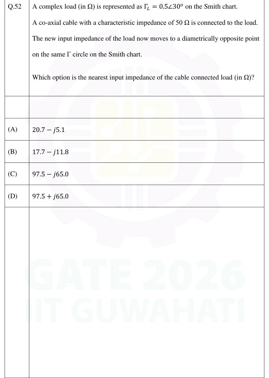
To convert an impedance to an admittance, go to the diametrically opposite point on the same circle (180∘, which is a λ/4 move), because y=1/z corresponds to −Γ.
For the distance from the load to the first voltage minimum, rotate clockwise from zL to the horizontal axis left of the centre; for the first maximum, to the axis right of the centre.
On a lossy line the point spirals inward toward the centre as you move toward the generator, since ∣Γ∣ falls as e−2αd.
Reading the chart as an admittance chart. Plot y=g+jb on the same circles, which are then constant-g circles and constant-b arcs. In this reading the upper half means capacitive susceptance (b>0), the right end of the axis is y→∞ (a short circuit) and the left end is y=0 (an open circuit); moving toward the generator is still clockwise. A short-circuited stub therefore starts at the right end: turning 90∘ clockwise from there (ℓ=λ/8) lands on y=−j1, the stub used in the matching example above.
EXAM TIP
Any Smith chart result can be checked by calculation: rotate with Γ(d)=ΓLe−j2βd, then convert with z=(1+Γ)/(1−Γ). For a numerical-answer question, compute rather than read the chart; a chart reading is only as precise as the drawing.
EXAM TIP
The admittance point lies 180∘ round the chart, which is a λ/4 move along the line. That is the Smith chart picture of the quarter-wave inverter zin=1/zL.
S-parameters of a two-port
At microwave frequencies ideal opens and shorts are hard to make, so a network is described by how it scatters travelling waves when its ports are terminated in matched loads. Convention: every port uses the same real reference impedance Z0; with peak phasors, ∣an∣2/2 is the power incident on port n and ∣bn∣2/2 the power leaving it. The definitions extend to any number of ports; the two-port is written out here.
INCIDENT AND REFLECTED WAVE VARIABLES
an=Z0Vn+,bn=Z0Vn−
an enters port n,bn leaves it. The net time-average power into port n is 21(∣an∣2−∣bn∣2).
S11 is the reflection coefficient at port 1 with port 2 terminated in Z0 (matched, not shorted); S21 is the transmission coefficient from port 1 to port 2 under the same condition.
INPUT REFLECTION COEFFICIENT WITH AN ARBITRARY LOAD
Γin=S11+1−S22ΓLS12S21ΓL
ΓL is the reflection coefficient of the load on port 2, referred to Z0.Γin=S11 only when ΓL=0. Looking back into port 2 with a source of reflection coefficient Γs on port 1, Γout=S22+S12S21Γs/(1−S11Γs).
All with port 2 matched. ∣S21∣2 is the fraction of the incident power delivered to the matched load on port 2.
RECIPROCITY
S12=S21,i.e. [S]=[S]T
Holds for linear networks built only from reciprocal elements (line sections, R, L, C, coupled coils and transformers), with the same real reference impedance at both ports. Fails for magnetically biased ferrite devices (isolators, circulators) and for active circuits such as amplifiers.
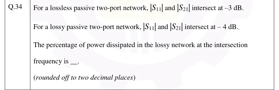
Each column carries unit power and different columns are orthogonal (equivalently, [S][S]∗T=[I], so the rows are too). For a lossless two-port this forces ∣S11∣=∣S22∣ and ∣S12∣=∣S21∣. Any passive network has ∣S11∣2+∣S21∣2≤1; the shortfall is the fraction of the power incident on port 1 that is dissipated inside the network (port 2 matched).
SERIES IMPEDANCE $Z$ BETWEEN THE PORTS
S11=S22=Z+2Z0Z,S21=S12=Z+2Z02Z0
Port 1 sees Z+Z0 when port 2 is matched.
SHUNT ADMITTANCE $Y$ ACROSS THE PORTS
S11=S22=2+YZ0−YZ0,S21=S12=2+YZ02
Here S21=1+S11 because the voltage is the same on both sides of a shunt element.
MATCHED LOSSLESS LINE SECTION AND REFERENCE-PLANE SHIFT
[S]=[0e−jβℓe−jβℓ0],Smn′=Smne−jβ(ℓm+ℓn)
A line of the reference impedance Z0 and length ℓ. Moving the reference plane at port n outward by a length ℓn of matched line changes only phases: S11′=S11e−j2βℓ1.
Properties of some standard networks (same reference impedance at every port)
Network
S-parameters (up to phase factors)
Reciprocal?
Lossless?
Matched lossless line section
S11=S22=0,∣S21∣=∣S12∣=1
yes
yes
Matched attenuator of A dB
S11=S22=0,∣S21∣=∣S12∣=10−A/20
yes
no
Series reactance Z=jX or shunt susceptance Y=jB
the two formulas above
yes
yes
Ideal isolator (passes port 1 to port 2)
S11=S22=S12=0,∣S21∣=1
no
no: power entering port 2 is absorbed
Ideal three-port circulator (1→2→3→1)
∣S21∣=∣S32∣=∣S13∣=1, all others 0
no
yes
WORKED EXAMPLE
A 50Ω resistor is connected in series between port 1 and port 2 of a 50Ω system. Find its S-parameters, state whether it is reciprocal and whether it is lossless, find the return loss and insertion loss, and account for all of the incident power.
▸ Solution
With port 2 terminated in 50Ω, port 1 sees 50+50=100Ω:S11=100+50100−50=31. By symmetry S22=31.
The voltage at port 1 is V1+(1+S11)=34V1+. The divider gives V2=21×34V1+=32V1+, and with port 2 matched V2=V2−, so S21=32 (the same as 2Z0/(Z+2Z0)=100/150). By symmetry S12=32.
Reciprocal, since S12=S21. Not lossless: ∣S11∣2+∣S21∣2=91+94=95<1.
Power balance: 91 of the incident power is reflected, 94 reaches the port-2 load, and the remaining 94 is dissipated in the series resistor. That is consistent: the resistor carries the same current as the 50Ω load and has the same resistance.
Return loss =−20log10(1/3)=9.54 dB; insertion loss =−20log10(2/3)=3.52 dB.
Answer:S11=S22=1/3,S12=S21=2/3; reciprocal but lossy; return loss 9.54 dB, insertion loss 3.52 dB; power split 1/9 reflected, 4/9 delivered, 4/9 dissipated.
EXAM TIP
Reciprocal and lossless are independent tests. Reciprocity is symmetry (S12=S21); losslessness is unitarity. A resistive attenuator is reciprocal but lossy; an ideal ferrite circulator is lossless but not reciprocal.
EXAM TIP
Use 20log10 on ∣Sij∣ (a wave-amplitude ratio) or 10log10 on ∣Sij∣2 (a power ratio); both give the same dB figure. Writing 10log10∣S21∣ halves the answer.
PREVIOUS-YEAR QUESTIONS
13 questions from the EC papers
Try each question first, then open the answer. We placed each question under a topic ourselves; the exam paper does not label topics.
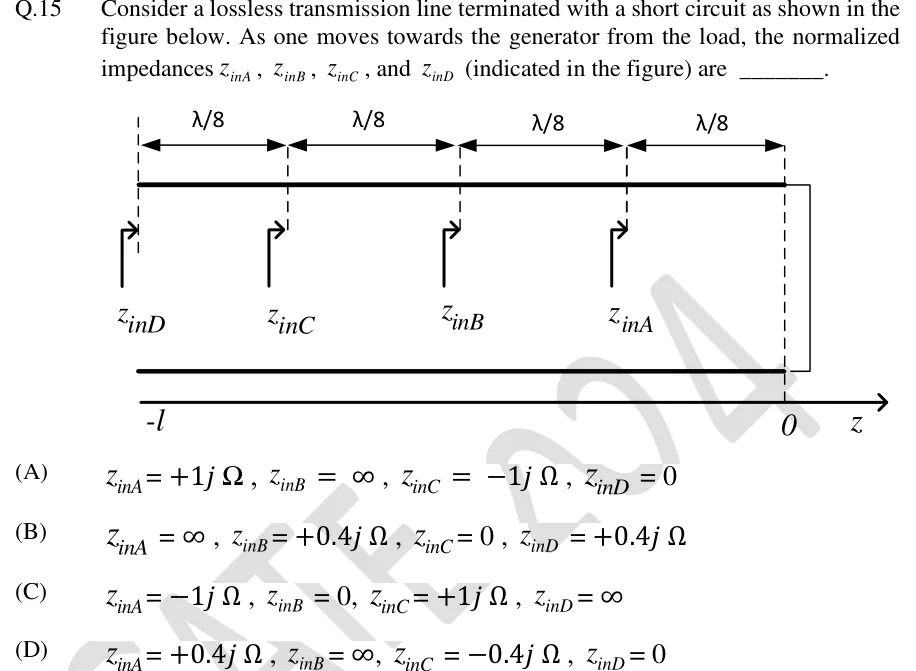
Consider a lossless transmission line terminated with a short circuit as shown in the figure below. As one moves towards the generator from the load, the normalized impedances zinA,zinB,zinC, and zinD (indicated in the figure) are ________.
Tap to open full sizeFigure from the GATE 2024 EC paper. It is part of the question.Figure description
A two-wire lossless transmission line drawn horizontally (two thick parallel lines). At the right end (z = 0) the two conductors are joined by a vertical wire, i.e. a short-circuit load. A z-axis runs left to right beneath the line, with the right end marked 0 and the left end marked -l. Vertical dashed lines divide the line into four equal segments, each labelled λ/8 with double-headed arrows along the top. Moving from the load (z = 0) towards the generator (left): the first dashed line (distance λ/8 from the load) is labelled z_inA, the second (distance λ/4) is labelled z_inB, the third (distance 3λ/8) is labelled z_inC, and the fourth, at the left end z = -l (distance λ/2), is labelled z_inD. Each label has a right-pointing bent arrow indicating the impedance looking towards the load.
A lossless transmission line with characteristic impedance Z0=50Ω is terminated with an unknown load. The magnitude of the reflection co-efficient is ∣Γ∣=0.6. As one moves towards the generator from the load, the maximum value of the input impedance magnitude looking towards the load (in Ω) is ________.
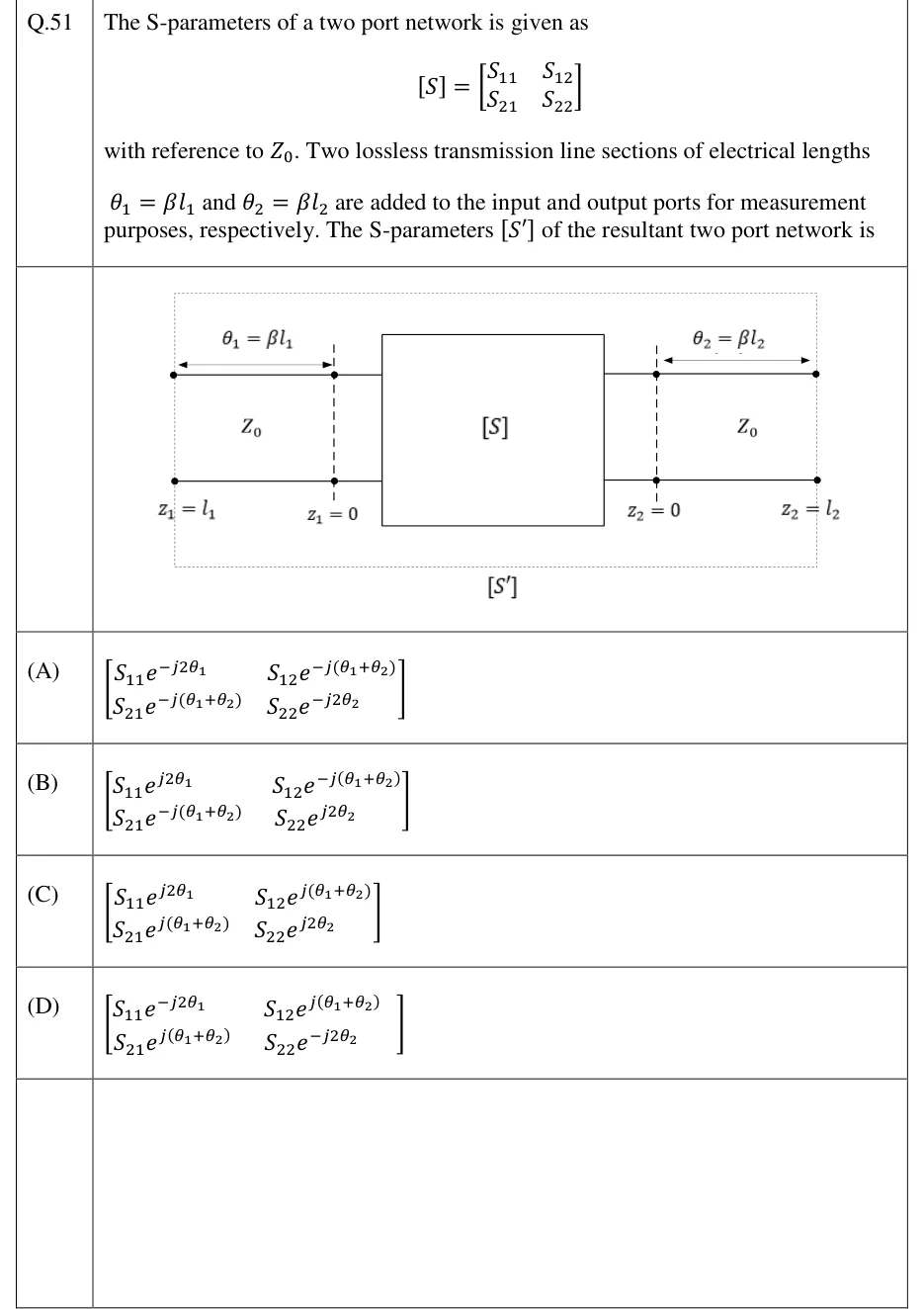
The S-parameters of a two port network is given as
[S]=[S11S21S12S22]
with reference to Z0. Two lossless transmission line sections of electrical lengths θ1=βl1 and θ2=βl2 are added to the input and output ports for measurement purposes, respectively. The S-parameters [S′] of the resultant two port network is
Tap to open full sizeFigure from the GATE 2023 EC paper. It is part of the question.Figure description
A box labelled [S] in the centre (the original two-port). On its left, a two-wire transmission line section of characteristic impedance Z_0 is attached to port 1. Its outer (far-left) terminals are marked z_1 = l_1 and the terminals where it meets the [S] box are marked z_1 = 0 (dashed vertical reference line). A double-headed arrow above this left section is labelled theta_1 = beta l_1. On the right, a second two-wire line section of characteristic impedance Z_0 is attached to port 2. The terminals at the box are marked z_2 = 0 (dashed vertical reference line) and the outer (far-right) terminals are marked z_2 = l_2. A double-headed arrow above it is labelled theta_2 = beta l_2. A dotted rectangle encloses both line sections and the [S] box, and is labelled [S'] beneath it: the new two-port whose reference planes are at z_1 = l_1 and z_2 = l_2.
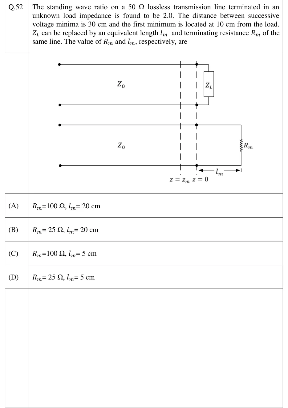
The standing wave ratio on a 50 Ω lossless transmission line terminated in an unknown load impedance is found to be 2.0. The distance between successive voltage minima is 30 cm and the first minimum is located at 10 cm from the load. ZL can be replaced by an equivalent length lm and terminating resistance Rm of the same line. The value of Rm and lm, respectively, are
Tap to open full sizeFigure from the GATE 2023 EC paper. It is part of the question.Figure description
Two transmission lines, one drawn above the other. Each is a pair of horizontal parallel wires labelled Z_0, with open input terminals (dots) at the left end. Upper line: its wires end at the plane z = 0 (dots on both wires) and are joined there to a box labelled Z_L. Lower line: the same line Z_0 carries on past the plane z = 0 for a further length l_m (a double-headed arrow from z = 0 to the right end, labelled l_m) and ends in a resistor (zigzag symbol) labelled R_m. Two vertical dashed lines cross both lines. The right one is at z = 0, the load plane of the upper line. The left one, a short way towards the input, is labelled z = z_m. The labels z = z_m and z = 0 are printed under the lower line. Not to scale.
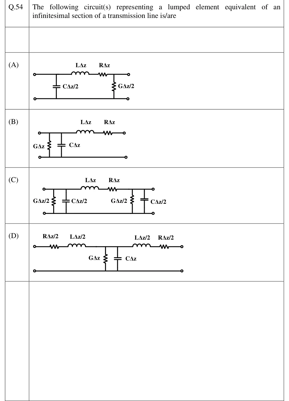
The following circuit(s) representing a lumped element equivalent of an infinitesimal section of a transmission line is/are
Tap to open full sizeFigure from the GATE 2023 EC paper. It is part of the question.Figure description
Each option is a two-port with a top (signal) wire and a bottom (return) wire, input terminals on the left and output terminals on the right. (A) Top wire: series inductor L Δ z followed by series resistor R Δ z. Shunt branches: a capacitor C Δ z/2 across the input side (before the inductor) and a resistor (conductance) G Δ z/2 across the output side (after the resistor). There is no shunt G at the input and no shunt C at the output. (B) Shunt conductance G Δ z and shunt capacitor C Δ z in parallel across the input terminals, then series inductor L Δ z and series resistor R Δ z on the top wire to the output (L-section). (C) Shunt G Δ z/2 and C Δ z/2 in parallel across the input, series L Δ z and R Δ z on the top wire, then shunt G Δ z/2 and C Δ z/2 in parallel across the output (pi-section). (D) Top wire: series R Δ z/2, series L Δ z/2, then at the midpoint a shunt G Δ z in parallel with C Δ z to the bottom wire, then series L Δ z/2 and series R Δ z/2 to the output (T-section).
(A)
Figure — series LΔz and RΔz; shunt CΔz/2 only at the input side and shunt GΔz/2 only at the output side
(B)
Figure — shunt GΔz∥CΔz at the input, followed by series LΔz and RΔz
(C)
Figure — shunt GΔz/2∥CΔz/2 at the input, series LΔz and RΔz, shunt GΔz/2∥CΔz/2 at the output
(D)
Figure — series RΔz/2 and LΔz/2, shunt GΔz∥CΔz at the middle, series LΔz/2 and RΔz/2
A transmission line of length 3λ/4 and having a characteristic impedance of 50Ω is terminated with a load of 400Ω. The impedance (rounded off to two decimal places) seen at the input end of the transmission line is ________ Ω.
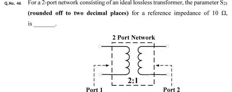
For a 2-port network consisting of an ideal lossless transformer, the parameter S21(rounded off to two decimal places) for a reference impedance of 10Ω, is ________.
Tap to open full sizeFigure from the GATE 2020 EC paper. It is part of the question.Figure description
A dashed rectangle labelled "2 Port Network" at the top holds an ideal transformer drawn as two coupled coils side by side: the left (primary) coil connects to a top-left and a bottom-left terminal (open circles), and the right (secondary) coil connects to a top-right and a bottom-right terminal (open circles). The turns ratio "2:1" (primary: secondary) is printed below the coils inside the dashed box. No polarity dots are drawn. On the left, a dashed bracket with an arrow pointing right into the left terminal pair is labelled "Port 1". On the right, a dashed bracket with an arrow pointing left into the right terminal pair is labelled "Port 2".
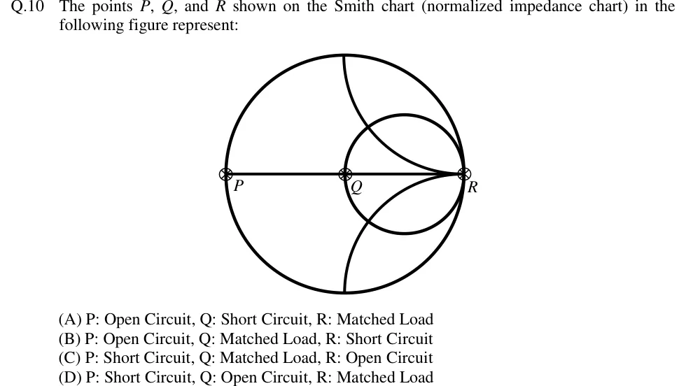
The points P,Q, and R shown on the Smith chart (normalized impedance chart) in the following figure represent:
Tap to open full sizeFigure from the GATE 2018 EC paper. It is part of the question.Figure description
A normalized-impedance Smith chart drawn in outline. The outer unit circle (| Γ | = 1) is shown, with a horizontal diameter (the real axis, x = 0) running from the leftmost point to the rightmost point. A smaller circle passes through the chart centre and the rightmost point (the r = 1 constant-resistance circle). Two arcs run from the top and bottom of the outer circle to the rightmost point (the x = +1 arc in the upper half and the x = -1 arc in the lower half). Three points are marked with a circled cross: P at the leftmost end of the horizontal diameter, Q at the centre of the chart (where the r = 1 circle meets the real axis on its left side), and R at the rightmost end of the horizontal diameter, where all the circles and arcs meet.
(A)
P: Open Circuit, Q: Short Circuit, R: Matched Load
(B)
P: Open Circuit, Q: Matched Load, R: Short Circuit
(C)
P: Short Circuit, Q: Matched Load, R: Open Circuit
(D)
P: Short Circuit, Q: Open Circuit, R: Matched Load
A lossy transmission line has resistance per unit length R=0.05Ω/m. The line is distortionless and has characteristic impedance of 50Ω. The attenuation constant (in Np/m, correct to three decimal places) of the line is ______.
A lossless 75Ω line of length 0.375λ is short-circuited at its far end. At the operating frequency, its input impedance is
(A)
+j75Ω (inductive)
(B)
−j75Ω (capacitive)
(C)
an open circuit
(D)
+j181Ω (inductive)
▸ Answer and solution
Answer: (B)
βℓ=2π×0.375=3π/4=135∘.
Zin=jZ0tanβℓ=j75tan135∘=−j75Ω: capacitive, as expected for a short stub between λ/4 and λ/2.
Smith chart check: start at the short, Γ=−1, and turn 720∘×0.375=270∘ clockwise, landing at Γ=−j, i.e. z=(1−j)/(1+j)=−j1.
Option D is the value obtained by wrongly using βℓ=67.5∘.
PRACTICE 22 marks · NAT
A lossless 50Ω line is terminated in a load ZL=30−j40Ω. The load is to be matched by cutting the main line at the voltage minimum nearest to the load and inserting a quarter-wave section of lossless line there. The characteristic impedance of the quarter-wave section, in Ω, is ______ (round off to two decimal places).
▸ Answer and solution
Answer:28.87 (accepted range ±0.05)
ΓL=80−j40−20−j40=802+402(−20−j40)(80+j40)=8000−j4000=−j0.5, so ∣ΓL∣=0.5 and θL=−90∘.
First minimum where θL−2βd=−180∘: 2βd=90∘, so dmin=90/720λ=0.125λ.
VSWR S=0.51.5=3, so the line impedance at the minimum is Z0/S=16.67Ω. Check at d=λ/8 (tanβd=1):Zin=5050+j(30−j40)30−j40+j50=5090+j3030+j10=16.67Ω.
ZT=50×16.67=350=28.87Ω.
PRACTICE 32 marks · MSQ
A two-port network, characterised with a 50Ω reference impedance at both ports, has the scattering matrix [S]=[0.6j0.8j0.80.6]. Which of the following statements is/are correct?
(A)
The network is reciprocal.
(B)
The network is lossless.
(C)
With port 2 terminated in a matched load, the return loss at port 1 is approximately 4.44 dB.
(D)
With port 2 terminated in a matched load, the insertion loss from port 1 to port 2 is approximately 0.97 dB.
▸ Answer and solution
Answer: (A), (B), (C)
S12=S21=j0.8, so the network is reciprocal: A is correct.
Column 1: ∣0.6∣2+∣j0.8∣2=0.36+0.64=1; column 2 is the same. Orthogonality: S11∗S12+S21∗S22=0.6(j0.8)+(−j0.8)(0.6)=0. The matrix is unitary, so the network is lossless: B is correct.
Return loss =−20log100.6=4.44 dB: C is correct.
Insertion loss =−20log100.8=1.94 dB. The figure 0.97 dB comes from wrongly using 10log10∣S21∣: D is incorrect.
PRACTICE 42 marks · NAT
A lossless 50Ω line is terminated in a 200Ω resistor. The load is to be matched with a single short-circuited shunt stub made of the same 50Ω line. For the solution in which the stub is attached closest to the load, the length of the shortest such stub, in wavelengths, is ______ (round off to three decimal places).
▸ Answer and solution
Answer:0.094 (accepted range ±0.002)
zL=200/50=4, so yL=0.25.
With t=tanβd:y(d)=1+j0.25t0.25+jt=1+0.0625t2(0.25+0.25t2)+j0.9375t.
Real part =1:0.25+0.25t2=1+0.0625t2, so 0.1875t2=0.75 and t=±2 (that is, ±r with r=4).
Closest to the load: t=+2,βd=tan−12=63.43∘, d=63.43/360λ=0.176λ. There the imaginary part is 1.250.9375×2=1.5, so y=1+j1.5.
The stub must supply −j1.5:−jcotβℓ=−j1.5, so tanβℓ=1/1.5 and βℓ=33.69∘.
ℓ=33.69/360λ=0.094λ. (The other solution, at d=0.324λ, needs a 0.406λ stub.)
PRACTICE 51 mark · NAT
A lossless 50Ω line is terminated in a load ZL=25+j25Ω. The voltage standing wave ratio on the line is ______ (round off to two decimal places).