IAE Academy

GATE CS

ALU design and the control unit

Hardwired and microprogrammed

A CPU executes an instruction as a sequence of register transfers. The ALU does the arithmetic and logic. Its adder is either ripple-carry (little hardware, delay grows as n) or carry look-ahead (more hardware; delay is constant for a single level with unlimited fan-in, and O(log n) when built in levels). The control unit produces the control signals for each step, either from logic wired around a state counter (hardwired: fast but rigid) or by reading microinstructions from a control memory (microprogrammed: flexible, slower). Microinstructions can be horizontal (one bit per signal) or encoded (vertical), and control-memory size = number of words × word width.

5 previous-year questions · 5 solved · 5 practice questions

ALU Design: Adders, Subtraction and Carry Look-Ahead

The Arithmetic and Logic Unit (ALU) performs arithmetic operations (add, subtract, increment, decrement) and logic operations (AND, OR, XOR, NOT, shifts). An -bit ALU is commonly built from identical bit-slices. In each slice, a multiplexer driven by function-select lines chooses which operation's result reaches the output, so select lines can choose among at most operations. Subtraction is done by adding the 2's complement, so the adder is the core of the arithmetic side and its carry chain sets the ALU's speed. The two adder designs to know are the ripple-carry adder (little hardware, slow) and the carry look-ahead adder (more hardware, fast).

Convention used throughout (unless a question says otherwise): numbers are in 2's complement. Bits are numbered (LSB) to (MSB), is the carry into bit 0 and is the final carry-out. A full adder (FA) takes and produces and a fixed delay after its inputs are stable. All delays are worst case. When delays are counted in gates, each gate (including XOR) counts as 1 gate delay and fan-in is unlimited. If a question gives its own figures, use those.

FULL ADDER EQUATIONS

One bit-slice of any adder. Both outputs need all three inputs to be stable.

SUBTRACTION AND OVERFLOW (2'S COMPLEMENT)

An adder/subtractor passes each through an XOR gate with a mode line and sets : adds and subtracts. signals signed (2's complement) overflow. For unsigned numbers, after an addition means the result does not fit in bits. After a subtraction done as , means (no borrow).

Ripple-carry adder (RCA): full adders are cascaded, with the carry-out of bit feeding the carry-in of bit . In the worst case (for example , ), a carry generated at bit 0 must ripple through every stage, so the carry chain is the critical path.

RIPPLE-CARRY ADDER WORST-CASE DELAY

is one FA's carry delay and is its sum delay, measured from when its carry-in is stable (its , are already stable). If one figure is given for both outputs, both times equal . The delay grows linearly with .

Carry look-ahead adder (CLA): instead of waiting for the carry to ripple, every carry is written directly in terms of and per-bit generate and propagate signals, so all carries can be formed at once.

GENERATE, PROPAGATE AND SUM

: bit produces a carry whatever is. : bit passes an incoming carry on to . Some texts use . The carry equations below still hold with that choice, but the sum can then no longer be formed as .

CARRY RECURRENCE AND ITS LOOK-AHEAD EXPANSION

Each expanded carry is a two-level AND-OR expression in the 's, 's and , so every carry is ready 2 gate delays after the , signals, whatever its position. The cost is fan-in: has product terms and its largest AND gate has inputs.

SINGLE-LEVEL CLA DELAY (CONVENTION ABOVE)

This is independent of only because fan-in is assumed unlimited. If a question counts an XOR as more than one gate delay, substitute its figure in the first and last terms.

BLOCK (GROUP) GENERATE AND PROPAGATE FOR A 4-BIT BLOCK

Fan-in limits force wide adders to be built from -bit CLA blocks. Each block's , take 2 gate delays after the bit-level , . A second-level look-ahead unit applies the same carry equations to the block signals, giving the carry into every block at once instead of rippling between blocks. With a fixed block size , the number of look-ahead levels grows as , so the delay grows as .

How to solve a CLA timing question

  1. Draw the chain of stages: bit-level , → block , (if there is a second level) → look-ahead unit giving the carry into each block → carries inside the block → sum bits.

  2. Take each stage's delay from the question. If none is given, use the convention above: 1 gate delay for and , 2 for any AND-OR carry or group level, 1 for the final XOR.

  3. A stage can start only when its latest input is stable. For example, a block's internal carries need both its own , and its carry-in, and the carry-in is usually the later one.

  4. The worst case is the path to the sum bits of the block whose carry-in arrives last. Stages that run in parallel in different blocks are never added together.

EXAM TIP

Some questions combine ripple-carry blocks with a look-ahead unit between blocks, and give one delay per full adder and a different delay per look-ahead level. Check which figure applies to which stage before adding anything.

Datapath and Register Transfers

The datapath is the set of registers, buses, ALU and multiplexers that move and transform data. The control unit decides, cycle by cycle, which register loads, which register drives a bus and which ALU operation is performed. A typical datapath has general-purpose registers, a Memory Address Register (MAR), a Memory Data (Buffer) Register (MDR/MBR), the Program Counter (PC), the Instruction Register (IR), and one or more internal buses that connect them through the ALU.

A register transfer is written in micro-operation notation, for example MAR ← PC (copy PC into MAR) or AC ← AC + DR (add DR into the accumulator). A transfer that completes in one clock cycle is a micro-operation. Every machine instruction runs as a sequence of micro-operations, and producing that sequence is the control unit's job, whether it is hardwired or microprogrammed.

Register-transfer notation

  1. R2 ← R1: the content of R1 is copied into R2 and R1 is unchanged.

  2. A comma joins micro-operations done in the SAME clock cycle, for example MAR ← PC, PC ← PC + 1. This is possible only if the hardware has separate paths for them (here, a PC incrementer that does not use the shared bus).

  3. P: R2 ← R1 means the transfer happens only when the control condition P is 1, for example T5 · D_ADD: AC ← AC + MDR (at timing step T5, and only for an ADD instruction).

  4. On a single shared bus, only ONE register can drive the bus in a cycle, but any number of registers can load from it in that cycle. So R2 ← R1 over the bus takes one cycle, and two transfers from different sources need two cycles.

EXAM TIP

To count cycles on a single-bus datapath, count how many different sources must drive the bus, one per cycle. One value on the bus can load several destinations in the same cycle.

The Instruction Cycle

Every instruction runs through the same phases: Fetch → Decode → (Operand fetch, if needed) → Execute → (Interrupt check). The control unit steps through these phases, issuing the correct control signals in each cycle, and then returns to Fetch.

Typical micro-operations (single-bus, accumulator machine)

  1. Fetch: MAR ← PC; then MDR ← M[MAR], PC ← PC + 1 (the increment uses a separate incrementer); then IR ← MDR.

  2. Decode: the opcode bits of IR are decoded to select the execute sequence. This is combinational and needs no register transfer of its own.

  3. Operand fetch with indirect addressing: MAR ← IR(address); then MDR ← M[MAR]; then MAR ← MDR (MAR now holds the effective address).

  4. Execute, for example ADD: MDR ← M[MAR]; then AC ← AC + MDR.

  5. Interrupt check: at the end of the instruction, if an interrupt is pending and enabled, the control unit saves the PC and transfers control to the interrupt handler instead of fetching the next instruction.

A hardwired and a microprogrammed control unit can implement exactly the same micro-operation sequence for an instruction set. They differ only in how the control signals for each step are produced.

Hardwired Control Unit

A hardwired control unit produces control signals directly from combinational logic whose inputs are the decoded opcode (from IR), the current timing state () and the condition flags. It is a finite state machine (Moore or Mealy): a state register or sequence counter records the current step of the instruction cycle, and logic computes the next state and the control outputs.

Structure of a hardwired control unit

  1. A sequence counter (or state register) steps through and is cleared to after an instruction's last step (or on an interrupt).

  2. An opcode decoder turns the IR opcode into one-hot lines such as D_ADD or D_STORE.

  3. Each control signal is an OR of AND terms of {timing state} · {decoded opcode} · {flags}. For example, in the ADD sequence of the worked example below, MAR is loaded at T0 for every instruction and at T3 for ADD, so MAR_load = T0 + T3 · D_ADD + … (one term for each place it is used).

  4. The counter is cleared at the end of each instruction's sequence, so instructions of different lengths simply use different numbers of timing states.

Hardwired vs microprogrammed control

Aspect

Hardwired control

Microprogrammed control

Implementation

Logic and a state counter wired to the control lines

Control words (microinstructions) stored in a control memory, read out and applied each step

Speed

Faster: no control-memory read in each step

Slower: each step includes a control-memory access

Modifying the instruction set

Hard: the logic must be redesigned

Easy: rewrite the microprogram

Design regularity

Irregular logic; harder to design and debug for large instruction sets

Regular and systematic; suits large, complex instruction sets

Extra hardware

No control memory

Control memory plus a control address register and sequencing logic

Typical use

RISC and speed-critical designs

CISC designs with large instruction sets

EXAM TIP

Timing signals may be produced by a ring counter (one flip-flop per state, one-hot) instead of a binary counter and decoder. It is the same hardwired model with a different state encoding.

Microprogrammed Control Unit

A microprogrammed control unit stores the control signals for each step as a bit pattern called a microinstruction, held in a control memory (control store), usually a ROM. The sequence of microinstructions that implements one machine instruction is its microprogram. A control address register (CAR, also called the micro-program counter, μPC) holds the address of the current microinstruction.

Structure

  1. Control Address Register (CAR / μPC): the address of the current microinstruction.

  2. Control memory: one word per microinstruction.

  3. Control buffer/data register: holds the microinstruction just read. Its fields drive the control lines and the next-address logic.

  4. Sequencing logic: chooses the next CAR value. The choices are CAR + 1 (the next step of the same microprogram); a branch to the first microinstruction of a new machine instruction, found by mapping the opcode; or a conditional branch on a status flag, using a condition-select field and a next-address field.

Mapping: after a fetch, the opcode must be converted into the control-memory address of the first microinstruction of that instruction's microprogram. This is done by a mapping function, for example the opcode bits placed in fixed positions of the address, or a lookup ROM. It plays the role that the opcode decoder plays in hardwired control.

CONTROL MEMORY SIZE

is the number of words (microinstructions) and is the width of one microinstruction. When a question gives the number of address bits of the CAR instead, . Convert to bytes by dividing by 8, and to KB with K = .

NEXT-ADDRESS AND CONDITION-SELECT FIELD WIDTHS

is the number of control-memory words that must be addressable. is the number of branch choices the field must select among, counting 'unconditional' (or 'no branch') as a choice when the question includes it.

Horizontal and Vertical Microinstructions

The control field of a microinstruction can be encoded in different ways. Encoding trades control-memory width against decoding hardware and parallelism.

Horizontal vs vertical microinstruction format

Aspect

Horizontal

Vertical (encoded)

Encoding

One bit per control signal; any combination can be active together

Signals are encoded into fields; a decoder produces the actual control lines

Control-field width

One bit per signal (wide)

A field that selects one of choices needs bits (narrow)

Parallelism

High: many micro-operations in one microinstruction

Low: only one signal per encoded field can be active

Decoding

None needed

A decoder per field, adding a small delay

Microinstructions per machine instruction

Fewer

Often more

Control memory

Wider words

Narrower words, though often more of them

Most practical designs are partially encoded. Signals that can never be active together are grouped into fields, each field is decoded separately, and signals that must be able to act together are placed in different fields. This lies between fully horizontal and fully vertical formats.

CONTROL-FIELD WIDTH: HORIZONTAL VS ENCODED

Group holds mutually exclusive signals. The is the code for 'none of this group active'. Drop it (use ) only if the question says exactly one signal of the group is always active, or says no-operation need not be encoded.

Computing a microinstruction's width

  1. For each encoded field, count the choices it must represent (its signals, plus 'none' if needed) and take bits.

  2. Add one bit for each signal kept unencoded (horizontal).

  3. Add the condition-select bits and the next-address bits ().

  4. Multiply the total width by the number of words for the control-memory size, then convert to bytes or KB as asked (K = ).

EXAM TIP

independent signals that may be active together need bits. If at most one of them can be active at a time, an encoded field needs only bits, or if 'none' is never required.

Worked Examples

WORKED EXAMPLE

A CPU has one internal bus that connects all registers and the ALU. Only one register can drive the bus in a clock cycle, and loads happen at the end of the cycle from the value on the bus. The ALU takes its operands from two input latches X and Y, and its output can drive the bus directly. How many clock cycles does R3 ← R1 + R2 take, and what happens in each?

Solution
  1. Both operands must be in the ALU's input latches before it can add. Only one register can drive the bus per cycle, so R1 and R2 need separate cycles.

  2. Cycle 1: R1 drives the bus and X loads it (X ← R1).

  3. Cycle 2: R2 drives the bus and Y loads it (Y ← R2).

  4. Cycle 3: the ALU drives the bus with X + Y and R3 loads it (R3 ← X + Y). Only one source (the ALU) uses the bus in this cycle.

  5. Variant: in the common design where one ALU input comes straight from the bus and the result goes into an output register Z, the steps are Y ← R1, then Z ← Y + R2, then R3 ← Z. That is also 3 cycles.

Answer: 3 clock cycles: X ← R1; Y ← R2; R3 ← X + Y.

WORKED EXAMPLE

A hardwired control unit runs a direct-addressing ADD as follows. T0: MAR ← PC. T1: MDR ← M[MAR], PC ← PC + 1. T2: IR ← MDR (decoding is combinational and takes no extra cycle). T3: MAR ← IR(address). T4: MDR ← M[MAR]. T5: AC ← AC + MDR, after which the counter clears to T0. AC is loaded only by ADD, and D_ADD is the decoded ADD line. Write the expression for AC_load.

Solution
  1. AC must load exactly at the step where AC ← AC + MDR happens, and only for ADD.

  2. In the given sequence that step is T5.

  3. So AC_load must be 1 when the state is T5 AND the instruction is ADD.

  4. D_ADD is valid from T2 onward, once IR has been loaded, so it is valid at T5.

Answer: AC_load = T5 · D_ADD

WORKED EXAMPLE

A microprogrammed control unit has 256 words of control memory. Its control signals fall into three groups of mutually exclusive signals: 7, 12 and 3 signals. In each group, 'none active' must also be possible. A branch field selects among 4 status conditions or 'unconditional'. Find the microinstruction width (a) with the groups encoded and (b) fully horizontal.

Solution
  1. Encoded groups: , , , so the control field is 9 bits.

  2. Condition select: 5 choices, so bits.

  3. Next address: bits.

  4. (a) Encoded width = 9 + 3 + 8 = 20 bits.

  5. (b) Horizontal control field = 7 + 12 + 3 = 22 bits, so the width = 22 + 3 + 8 = 33 bits.

Answer: (a) 20 bits, (b) 33 bits

PREVIOUS-YEAR QUESTIONS

5 questions from the CS papers

Try each question first, then open the answer. We placed each question under a topic ourselves; the exam paper does not label topics.

See these papers in full: GATE CSE 2025 Set 1 · GATE CSE 2025 Set 2 · GATE CSE 2022 · GATE CSE 2020

GATE 2025 CS1 Q.27

GATE 2025 · CS1Q.27 · 1 mark · MSQ

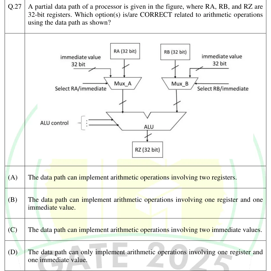
A partial data path of a processor is given in the figure, where RA, RB, and RZ are 32-bit registers. Which option(s) is/are CORRECT related to arithmetic operations using the data path as shown?

GATE 2025 CS1 question 27: A data path diagram.Tap to open full size
Figure from the GATE 2025 CS1 paper. It is part of the question.
Figure description

A data path diagram. Two input registers feed two 2:1 multiplexers: RA (32 bit) feeds down into Mux_A; RB (32 bit) feeds down into Mux_B. Mux_A also receives a second input labeled "immediate value, 32 bit" from the left, with a select line labeled "Select RA/immediate" feeding into Mux_A. Mux_B also receives a second input labeled "immediate value, 32 bit" from the right, with a select line labeled "Select RB/immediate" feeding into Mux_B. The outputs of Mux_A and Mux_B (each 32 bit, marked with slash-32 tick marks) both feed down into a single ALU block (drawn as a trapezoid). The ALU also receives multiple "ALU control" input lines from the left (drawn as a bus of several arrows). The ALU's output (32 bit) feeds down into register RZ (32 bit).

  1. (A)

    The data path can implement arithmetic operations involving two registers.

  2. (B)

    The data path can implement arithmetic operations involving one register and one immediate value.

  3. (C)

    The data path can implement arithmetic operations involving two immediate values.

  4. (D)

    The data path can only implement arithmetic operations involving one register and one immediate value.

Answer and solution
GATE 2025 CS1 Q.27: answer and solution

GATE 2020 CS Q.4

GATE 2020 · CSQ.4 · 1 mark · MCQ

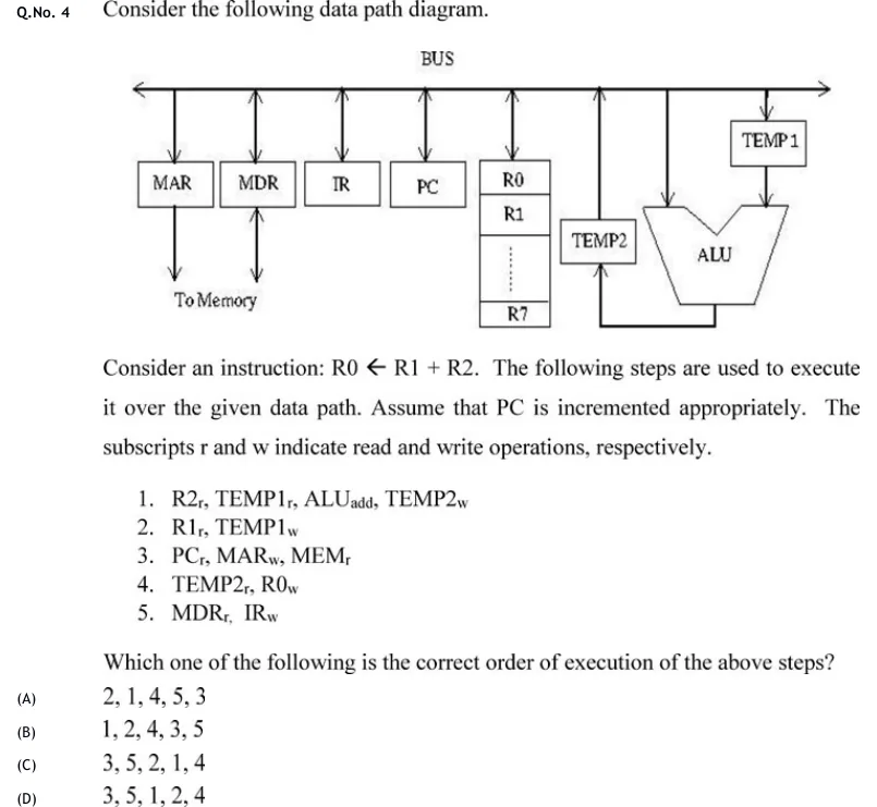
Consider the following data path diagram.

Consider an instruction: R0 ← R1 + R2. The following steps are used to execute it over the given data path. Assume that PC is incremented appropriately. The subscripts r and w indicate read and write operations, respectively.

1. R2r, TEMP1r, ALUadd, TEMP2w
2. R1r, TEMP1w
3. PCr, MARw, MEMr
4. TEMP2r, R0w
5. MDRr, IRw

Which one of the following is the correct order of execution of the above steps?

GATE 2020 CS question 4: A single-bus datapath diagram.Tap to open full size
Figure from the GATE 2020 CS paper. It is part of the question.
Figure description

A single-bus datapath diagram. A horizontal line labeled BUS runs across the top with double-headed (bidirectional) arrows connecting down to each block below it. From left to right, the blocks connected to the bus are: MAR (with a separate downward arrow labeled 'To Memory'), MDR (also connected 'To Memory' via the same downward line as MAR), IR, PC, a register file block containing R0, R1, R2,... (dots), R7 (i.e., R0 through R7 stacked vertically), TEMP2, and a V-shaped ALU block. Above and to the right, TEMP1 sits above the ALU and also connects down to the ALU. TEMP2 feeds into the left input of the ALU (via a line from TEMP2 down and into the ALU), and the ALU's output line loops back up into TEMP2's input from below/right (TEMP2's box has an arrow both up to bus and a feed line to ALU's left side coming from below). TEMP1 connects down into the ALU's right input. The ALU (V-shaped) output goes up to TEMP1's block position at top right. MAR and MDR each have an additional downward arrow labeled 'To Memory'.

  1. (A)

    2, 1, 4, 5, 3

  2. (B)

    1, 2, 4, 3, 5

  3. (C)

    3, 5, 2, 1, 4

  4. (D)

    3, 5, 1, 2, 4

Answer and solution
GATE 2020 CS Q.4: answer and solution

GATE 2020 CS Q.29

GATE 2020 · CSQ.29 · 2 marks · MCQ

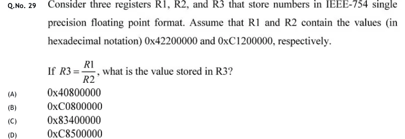
Consider three registers R1, R2, and R3 that store numbers in IEEE-754 single precision floating point format. Assume that R1 and R2 contain the values (in hexadecimal notation) 0x42200000 and 0xC1200000, respectively.

If , what is the value stored in R3?

  1. (A)

    0x40800000

  2. (B)

    0xC0800000

  3. (C)

    0x83400000

  4. (D)

    0xC8500000

Answer and solution
See the question in the paper
GATE 2020 CS Q.29: answer and solution

PRACTICE

5 questions to test yourself

PRACTICE 11 mark · MCQ

A 32-bit ripple-carry adder is built from 32 full adders. Each full adder produces both its sum and its carry-out 2 ns after its own inputs (including its carry-in) are stable. What is the worst-case time after the inputs are applied until both the final carry-out and the most significant sum bit are stable?

  1. (A)

    32 ns

  2. (B)

    64 ns

  3. (C)

    16 ns

  4. (D)

    2 ns

Answer and solution

Answer: (B)

  1. Number the bits 0 to 31. In the worst case a carry generated at bit 0 ripples through every stage.

  2. is stable 2 ns after , so is stable at ns.

  3. needs , which is stable at ns, so is stable at ns.

  4. Both are stable at 64 ns.

PRACTICE 22 marks · NAT

A 16-bit adder is built from four 4-bit carry look-ahead blocks joined by a second-level carry look-ahead unit. Count every gate (including XOR) as 1 gate delay. The bit-level , are ready 1 gate delay after the operands are applied. Each block's group signals , are ready 2 gate delays after its , . The second-level unit produces the carry into every block 2 gate delays after its inputs ( and all , ) are stable. Inside a block, the internal carries are ready 2 gate delays after both the block's , and its carry-in are stable, and the sum bits 1 gate delay after that. is available together with the operands. What is the worst-case delay, in gate delays, until all 16 sum bits are stable?

Answer and solution

Answer:

  1. , ready at 1.

  2. Block , ready at 1 + 2 = 3.

  3. The second-level unit gives the carry into blocks 1, 2 and 3 at 3 + 2 = 5. Block 0's carry-in is , available at 0.

  4. Blocks 1 to 3: their internal carries wait for the later of , (1) and the carry-in (5), so they are ready at 5 + 2 = 7, and the sums at 7 + 1 = 8.

  5. Block 0 finishes earlier: carries at 1 + 2 = 3, sums at 4.

  6. Worst case = 8 gate delays.

PRACTICE 32 marks · MSQ

Which of the following statements about a hardwired control unit are true?

  1. (A)

    Adding a new instruction generally requires redesigning the control logic or state diagram

  2. (B)

    For comparable technology, hardwired control is typically faster than microprogrammed control

  3. (C)

    The control signals are produced by reading a control memory addressed by a micro-program counter

  4. (D)

    Hardwired control is easier to modify for a new instruction than microprogrammed control

Answer and solution

Answer: (A), (B)

  1. A: In a hardwired unit, the control signals come from logic built around the opcode, the timing state and the flags. A new instruction means redesigning that logic. True.

  2. B: There is no control-memory read in each step, so for the same technology hardwired control is generally faster. True.

  3. C: Reading control words from a control memory addressed by a micro-program counter describes MICROPROGRAMMED control, not hardwired. False.

  4. D: Changing a hardwired unit means redesigning logic, whereas a microprogrammed unit only needs its microprogram rewritten. Hardwired control is therefore harder to modify, not easier. False.

PRACTICE 42 marks · NAT

A microprogrammed control unit holds 300 microinstructions. Each microinstruction specifies 40 independent control signals and has a next-address field that can point to any of the 300 microinstructions, and it has no other fields. With a fully HORIZONTAL format (one bit per control signal) and the minimum number of next-address bits, what is the width of one microinstruction in bits?

Answer and solution

Answer:

  1. Horizontal control field: 40 bits.

  2. Next address: bits, since .

  3. Width = 40 + 9 = 49 bits.

PRACTICE 51 mark · MCQ

A control memory holds 512 microinstructions, each 60 bits wide, with no padding. What is its size in bytes (1 byte = 8 bits)?

  1. (A)

    3840 bytes

  2. (B)

    3072 bytes

  3. (C)

    4096 bytes

  4. (D)

    30720 bytes

Answer and solution

Answer: (A)

  1. Total bits = 512 × 60 = 30720.

  2. Bytes = 30720 / 8 = 3840.

  3. Equivalently, 3840 / 1024 = 3.75 KB with K = .

OFFICIAL GATE 2027 SYLLABUS WORDING

Copied from the GATE 2027 syllabus; see all 2027 syllabi.

GATE CS

Design of arithmetic and logic unit (ALU). Design of control unit – hardwired and microprogrammed

Preparing in Kolkata? IAE Academy's course for GATE CSE.