IAE Academy

GATE EC

Carrier transport

Drift, diffusion, generation and recombination

Current in a semiconductor is the sum of drift (carriers pushed by an electric field) and diffusion (carriers spreading down a concentration gradient). Mobility, conductivity, the Einstein relation and the Hall effect describe drift, and they let you find carrier type, concentration and mobility from measurements. Generation and recombination set how long excess carriers survive (the lifetime) and how far they travel before disappearing (the diffusion length). The continuity equation combines drift, diffusion, generation and recombination in one equation, and its steady-state solutions (exponential for a long sample, near-linear for a short one) give the excess-carrier profiles behind diode, BJT and photodetector behaviour. Poisson's equation links the field to the space charge, and quasi-Fermi levels describe electron and hole populations separately once they are out of equilibrium. These are the tools used in every p-n junction problem.

9 previous-year questions · 9 solved · 6 practice questions

Drift Current, Mobility and Resistivity

An electric field exerts a force on free carriers. This gives them a net drift velocity on top of their random thermal motion, and the resulting current is drift current. How easily carriers drift, measured by their mobility, sets a semiconductor's conductivity.

DRIFT VELOCITY AND MOBILITY

Electrons drift opposite to (hence the minus sign) and holes drift along . are the electron and hole mobilities in . is the mean time between scattering events and is the conductivity effective mass. The linear relation holds only at low fields (see velocity saturation below).

DRIFT CURRENT DENSITY

C. With in and in V/cm, is in . Electron and hole drift currents both point along (conventional current), so they add.

CONDUCTIVITY AND RESISTIVITY

For a fully ionized, uncompensated extrinsic sample with doping much larger than , one term dominates: (n-type) or (p-type). In a compensated sample, use the net doping, e.g. when . The mobility is still reduced by all ionized impurities. For an intrinsic sample, . is the length along the current and the cross-section.

MINIMUM CONDUCTIVITY

This uses (thermal equilibrium, non-degenerate). Since in Si, the minimum lies at , i.e. in slightly p-type material, not at the intrinsic point. because .

Mobility is not a constant. Two scattering mechanisms limit it. Lattice (phonon) scattering grows with temperature. Ionized-impurity scattering grows with the ionized-dopant concentration and weakens as temperature rises, because faster carriers are deflected less. So falls as doping increases. Near and above room temperature, where lattice scattering dominates in lightly and moderately doped Si, falls as rises. At low temperature or in heavily doped material, impurity scattering dominates and can rise with . In Si, . Commonly used values for lightly doped Si at 300 K are about and ; use the values a question gives.

COMBINING SCATTERING MECHANISMS

Independent scattering mechanisms add as reciprocals (Matthiessen's rule), so the mechanism that gives the lower mobility dominates. is the total ionized-impurity concentration. The power laws are the idealized dependences; measured exponents differ somewhat.

Velocity saturation

  1. At low fields, (the linear region used above).

  2. As increases, grows more slowly than linearly, because scattering increases with carrier energy.

  3. At high fields (of the order of V/cm in Si), approaches a saturation velocity (of the order of cm/s for electrons in Si at 300 K; somewhat lower for holes). Beyond this, barely changes with : the ratio falls and the low-field mobility no longer applies.

  4. Velocity saturation caps the drift current a region can carry, and it limits the drain current of short-channel MOSFETs.

EXAM TIP

If a question gives resistivity or conductivity and one doping concentration, assume full ionization and single-carrier conduction. Only do this if the doping is much larger than and the question does not give both and (as it would for a compensated or near-intrinsic sample). In those cases keep both terms of .

Diffusion Current and the Einstein Relation

Wherever carrier concentration is non-uniform, random thermal motion produces a net flow of carriers from high to low concentration. This is diffusion current, and it flows even with zero electric field. Drift and diffusion can act together, and the total current is their sum.

DIFFUSION CURRENT DENSITY

are diffusion coefficients in . Both carriers diffuse from high to low concentration. Electrons are negative, so the electron diffusion current points up the electron gradient (it has the sign of ). Holes are positive, so the hole diffusion current points down the hole gradient (it has the sign of ).

TOTAL CURRENT DENSITY (1-D)

The drift-diffusion equations for each carrier type. They are the inputs to the continuity equation.

EINSTEIN RELATION

Holds for a non-degenerate semiconductor. It is derived in thermal equilibrium and used at low fields in the drift-diffusion model. V at K, often rounded to V or V. State the value you use, because the rounding shifts the third significant figure.

BUILT-IN FIELD FROM NON-UNIFORM DOPING

Conditions: thermal equilibrium (zero net current), full ionization, and quasi-neutrality ( or ). Drift must cancel diffusion, so a doping gradient produces a field. Example: gives a uniform field along .

EXAM TIP

The Einstein relation turns a mobility into a diffusion coefficient or back: . For example, gives with V. Check which the question intends before you round.

Hall Effect

Place a current-carrying sample in a transverse magnetic field and the magnetic force deflects the moving carriers to one side. This builds up a transverse (Hall) electric field, which in steady state exactly balances the magnetic force. The sign and size of the resulting Hall voltage give the majority-carrier type and its concentration. Combined with the conductivity, they also give the mobility.

HALL VOLTAGE AND HALL COEFFICIENT

flows along the sample length and is perpendicular to . is the sample thickness measured along , is the width across which is measured, and . does not depend on . For a fixed geometry, has opposite polarity for holes and for electrons, so the sign of (or ) identifies the majority carrier. These simple forms assume one dominant carrier type and take the Hall scattering factor as 1. From a measured : or .

HALL MOBILITY

Valid when one carrier type dominates. It combines the measured Hall coefficient and the measured conductivity to give the majority-carrier mobility.

EXAM TIP

Fix the units before substituting. Work fully in SI (metres, tesla, amperes, volts, coulombs): the concentration then comes out in , and multiplying by gives . Using a thickness in cm with in tesla gives a wrong answer.

Generation, Recombination, Lifetime and Diffusion Length

In thermal equilibrium, thermal generation (creating electron-hole pairs) and recombination (an electron falling back into a hole) balance exactly. For a non-degenerate semiconductor this gives . Light, or injection of carriers across a junction, disturbs the balance and creates excess carriers. When the disturbance is removed, the excess carriers decay back toward equilibrium at a rate set by the minority-carrier lifetime. In indirect-gap Si, recombination is mainly trap-assisted, through defect levels, which is why the lifetime depends strongly on defect density.

NET RECOMBINATION RATE (LOW-LEVEL INJECTION)

Valid for low-level injection, where the excess carrier density is much smaller than the majority-carrier density. and are the excess concentrations. In a neutral region with pair generation, . are the minority-carrier lifetimes; they depend on the material and its defects and are given as constants in problems.

UNIFORM GENERATION: STEADY STATE, DECAY AND PHOTOCONDUCTIVITY

Conditions: a uniformly illuminated n-type sample, low-level injection, and no concentration gradients (so no diffusion). The continuity equation then reduces to . is the optical generation rate in . Since , both carriers add to the conductivity.

DIFFUSION LENGTH

The characteristic distance a minority carrier diffuses before it recombines. In a long sample it is the decay length of the steady-state excess-carrier profile (see the continuity-equation section).

Quantities at a glance

Quantity

Symbol

Governs

Minority-carrier lifetime

How fast excess carriers recombine

Diffusion coefficient

How fast carriers spread by diffusion ()

Diffusion length

How far excess carriers travel before recombining ()

EXAM TIP

Low-level injection is the assumption behind the linear recombination rate and behind treating the majority-carrier concentration as unchanged. State it explicitly whenever you use it.

Continuity Equation and Steady-State Solutions

The continuity equation is conservation of carriers applied to each type separately. At any point, the rate of change of carrier concentration equals the net inflow from current, plus generation, minus recombination. It ties drift, diffusion, generation and recombination together, and an excess-carrier profile is found by solving it with the right boundary conditions.

CONTINUITY EQUATIONS (1-D)

and are the generation and recombination rates. The opposite signs come from the charge of each carrier: (electron flux) and (hole flux). Substituting the drift-diffusion expressions for and gives the minority-carrier equation below.

MINORITY-CARRIER (HOLE) EQUATION IN AN N-TYPE SAMPLE

Assumes uniform doping, a uniform field and low-level injection. is any externally driven generation, e.g. optical. With the drift term drops out. Setting the time derivative to zero gives the steady-state form.

STEADY-STATE SOLUTION, LONG SAMPLE (E = 0)

Conditions: no generation for , the excess concentration held at (e.g. by an injecting junction), and as (sample length much greater than ). The diffusion current decays with the same length as the profile.

STEADY-STATE SOLUTION, SAMPLE OF LENGTH W (E = 0)

The same equation with , as at an ohmic contact or a reverse-biased junction at . When , almost no carriers recombine in transit. The profile is then linear, and the diffusion current is nearly uniform. This is the short-base picture used for BJTs and short diodes.

WORKED EXAMPLE

An n-type Si bar has and hole lifetime . Excess holes are held at at , with , low-level injection, no other generation for , and a bar much longer than . Find (a) the diffusion length , (b) at , and (c) the hole diffusion current density at ( C).

Solution
  1. .

  2. Steady-state profile for a long bar: .

  3. At : , so .

  4. .

Answer: ; ; along .

Poisson's Equation and Quasi-Fermi Levels

Poisson's equation ties the electric field to the net charge in the semiconductor. It is needed wherever the field is set by the carrier and dopant distribution itself rather than applied from outside, as in a depletion region. Quasi-Fermi levels extend equilibrium Fermi statistics to describe the electron and hole populations separately once they are driven out of equilibrium by light or injection. That is exactly the situation the continuity equation deals with.

POISSON'S EQUATION (1-D)

. here is the space-charge density, not resistivity. is the semiconductor permittivity, with for Si and F/cm. With the depletion approximation ( inside the depletion region), it gives the field and potential profiles and the depletion width of a junction. For example, on the n-side of a step junction , so varies linearly with .

QUASI-FERMI LEVELS

Valid for a non-degenerate semiconductor. With no excess generation or injection, both reduce to the single equilibrium Fermi level (, ). Quoted values of for Si at 300 K range from about to . Use the value the question gives, and state it whenever a numerical answer depends on it.

CURRENT FROM THE QUASI-FERMI LEVEL GRADIENT

Equivalent to the drift-diffusion equations for a non-degenerate semiconductor with the Einstein relation. are in joules here; with energies in eV, multiply the right-hand side by . In thermal equilibrium the net current is zero, so the Fermi level is flat.

EXAM TIP

Under net generation or injection (illumination, forward bias), and . Across the depletion region of a junction forward-biased by (forward positive), the splitting equals , so at the depletion edges. Under reverse bias the order flips there: and , which means net generation. Use the sign of the splitting to check that a bias or illumination condition is physically consistent.

PREVIOUS-YEAR QUESTIONS

9 questions from the EC papers

Try each question first, then open the answer. We placed each question under a topic ourselves; the exam paper does not label topics.

See these papers in full: GATE ECE 2026 · GATE ECE 2025 · GATE ECE 2024 · GATE ECE 2023 · GATE ECE 2022 · GATE ECE 2020

GATE 2026 EC Q.64

GATE 2026 · ECQ.64 · 2 marks · NAT

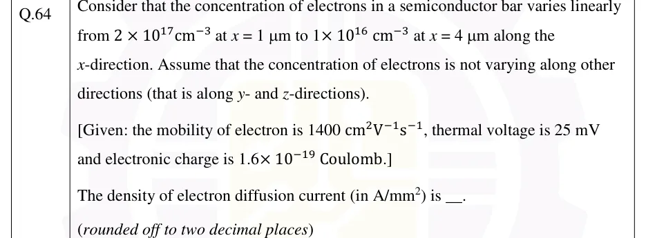
Consider that the concentration of electrons in a semiconductor bar varies linearly from at to at along the -direction. Assume that the concentration of electrons is not varying along other directions (that is along - and -directions).

[Given: the mobility of electron is , thermal voltage is and electronic charge is Coulomb.]

The density of electron diffusion current (in ) is ___.

(rounded off to two decimal places)

Answer and solution
See the question in the paper
GATE 2026 EC Q.64: answer and solution

GATE 2025 EC Q.46

GATE 2025 · ECQ.46 · 2 marks · MCQ

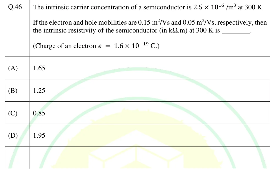
The intrinsic carrier concentration of a semiconductor is at 300 K. If the electron and hole mobilities are and , respectively, then the intrinsic resistivity of the semiconductor (in km) at 300 K is ________. (Charge of an electron .)

  1. (A)

    1.65

  2. (B)

    1.25

  3. (C)

    0.85

  4. (D)

    1.95

Answer and solution
See the question in the paper
GATE 2025 EC Q.46: answer and solution

GATE 2025 EC Q.48

GATE 2025 · ECQ.48 · 2 marks · MCQ

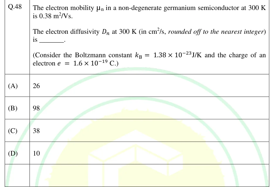
The electron mobility in a non-degenerate germanium semiconductor at 300 K is 0.38 m²/Vs.

The electron diffusivity at 300 K (in cm²/s, rounded off to the nearest integer) is ______.

(Consider the Boltzmann constant J/K and the charge of an electron C.)

  1. (A)

    26

  2. (B)

    98

  3. (C)

    38

  4. (D)

    10

Answer and solution
See the question in the paper
GATE 2025 EC Q.48: answer and solution

GATE 2024 EC Q.26

GATE 2024 · ECQ.26 · 1 mark · MSQ

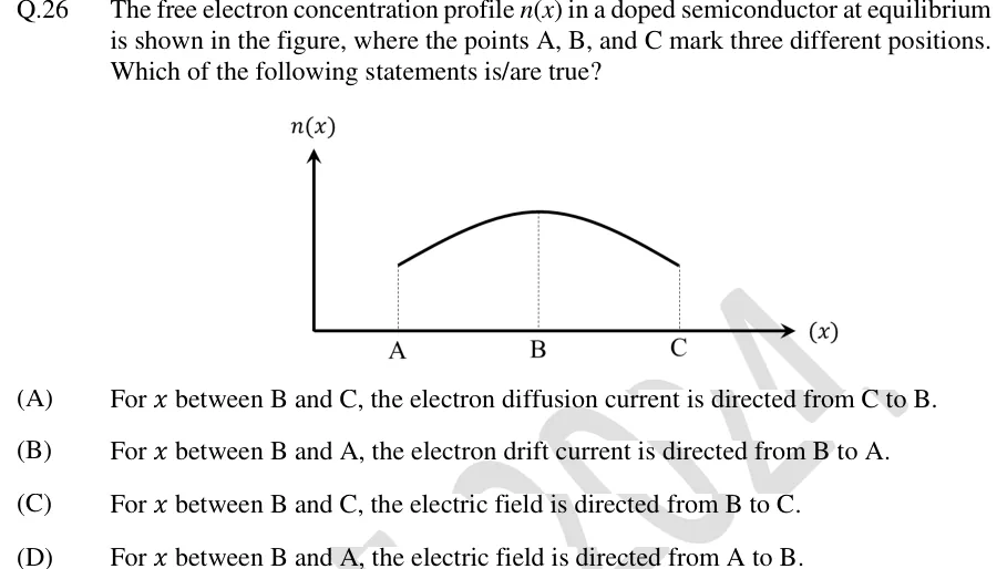
The free electron concentration profile in a doped semiconductor at equilibrium is shown in the figure, where the points A, B, and C mark three different positions. Which of the following statements is/are true?

GATE 2024 EC question 26: A plot of n(x) (vertical axis) versus x (horizontal axis).Tap to open full size
Figure from the GATE 2024 EC paper. It is part of the question.
Figure description

A plot of n(x) (vertical axis) versus x (horizontal axis). Over the marked interval the curve starts at a moderate value above point A, rises smoothly to a single maximum (peak) directly above point B, then falls smoothly back down to a lower value above point C. Points A, B, C lie on the x-axis in that left-to-right order (A leftmost, B in the middle below the peak, C rightmost), each joined to the curve by a dotted vertical line.

  1. (A)

    For x between B and C, the electron diffusion current is directed from C to B.

  2. (B)

    For x between B and A, the electron drift current is directed from B to A.

  3. (C)

    For x between B and C, the electric field is directed from B to C.

  4. (D)

    For x between B and A, the electric field is directed from A to B.

Answer and solution
GATE 2024 EC Q.26: answer and solution

GATE 2023 EC Q.56

GATE 2023 · ECQ.56 · 2 marks · NAT

In an extrinsic semiconductor, the hole concentration is given to be where is the intrinsic carrier concentration of . The ratio of electron to hole mobility for equal hole and electron drift current is given as ________ (rounded off to two decimal places).

Answer and solution
See the question in the paper
GATE 2023 EC Q.56: answer and solution

GATE 2022 EC Q.16

GATE 2022 · ECQ.16 · 1 mark · MCQ

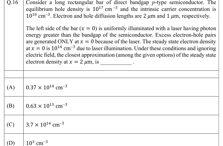
Consider a long rectangular bar of direct bandgap p-type semiconductor. The equilibrium hole density is and the intrinsic carrier concentration is . Electron and hole diffusion lengths are and , respectively.

The left side of the bar () is uniformly illuminated with a laser having photon energy greater than the bandgap of the semiconductor. Excess electron-hole pairs are generated ONLY at because of the laser. The steady state electron density at is due to laser illumination. Under these conditions and ignoring electric field, the closest approximation (among the given options) of the steady state electron density at , is ___________.

  1. (A)

  2. (B)

  3. (C)

  4. (D)

Answer and solution
See the question in the paper
GATE 2022 EC Q.16: answer and solution

GATE 2022 EC Q.47

GATE 2022 · ECQ.47 · 2 marks · MSQ

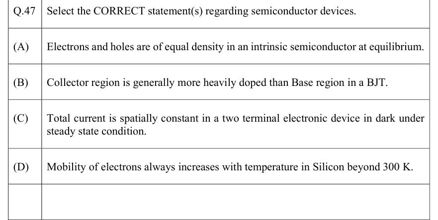
Select the CORRECT statement(s) regarding semiconductor devices.

  1. (A)

    Electrons and holes are of equal density in an intrinsic semiconductor at equilibrium.

  2. (B)

    Collector region is generally more heavily doped than Base region in a BJT.

  3. (C)

    Total current is spatially constant in a two terminal electronic device in dark under steady state condition.

  4. (D)

    Mobility of electrons always increases with temperature in Silicon beyond 300 K.

Answer and solution
See the question in the paper
GATE 2022 EC Q.47: answer and solution

GATE 2022 EC Q.56

GATE 2022 · ECQ.56 · 2 marks · NAT

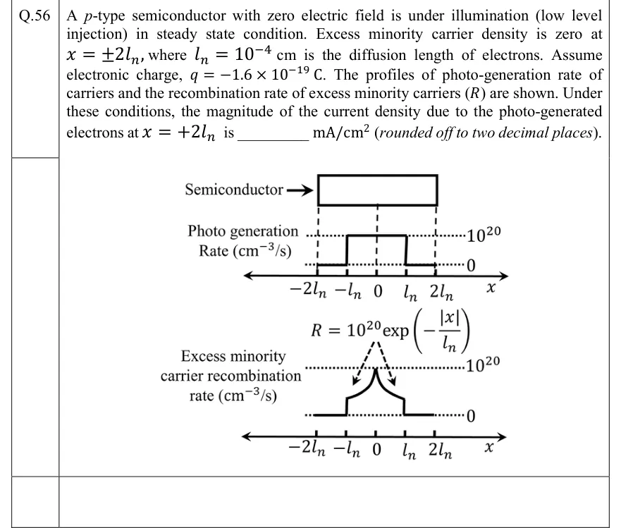
A -type semiconductor with zero electric field is under illumination (low level injection) in steady state condition. Excess minority carrier density is zero at , where cm is the diffusion length of electrons. Assume electronic charge, C. The profiles of photo-generation rate of carriers and the recombination rate of excess minority carriers () are shown. Under these conditions, the magnitude of the current density due to the photo-generated electrons at is ________ mA/cm (rounded off to two decimal places).

GATE 2022 EC question 56: A bar labelled 'Semiconductor' spans x = -2l_n to +2l_n.Tap to open full size
Figure from the GATE 2022 EC paper. It is part of the question.
Figure description

A bar labelled 'Semiconductor' spans x = -2l_n to +2l_n. Below it are two plots against x, each with ticks at -2l_n, -l_n, 0, l_n, 2l_n. (1) Photo generation rate (cm^-3/s): a rectangular pulse of height 10^20 for -l_n < x < l_n and 0 for l_n < |x| < 2l_n. (2) Excess minority carrier recombination rate (cm^-3/s), labelled R = 10^20 exp(-|x|/l_n): the curve peaks at 10^20 at x = 0 and decays symmetrically only as far as x = ±l_n. There it steps down vertically, from 10^20 e^-1, to 0, and it stays 0 for l_n < |x| < 2l_n.

Answer and solution
GATE 2022 EC Q.56: answer and solution

GATE 2020 EC Q.7

GATE 2020 · ECQ.7 · 1 mark · MCQ

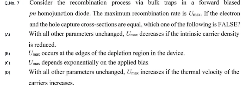
Consider the recombination process via bulk traps in a forward biased pn homojunction diode. The maximum recombination rate is . If the electron and the hole capture cross-sections are equal, which one of the following is FALSE?

  1. (A)

    With all other parameters unchanged, decreases if the intrinsic carrier density is reduced.

  2. (B)

    occurs at the edges of the depletion region in the device.

  3. (C)

    depends exponentially on the applied bias.

  4. (D)

    With all other parameters unchanged, increases if the thermal velocity of the carriers increases.

Answer and solution
See the question in the paper
GATE 2020 EC Q.7: answer and solution

PRACTICE

6 questions to test yourself

PRACTICE 11 mark · NAT

An n-type silicon sample has a fully ionized donor concentration () and resistivity at 300 K. Assume electron drift dominates conduction (the hole contribution is negligible) and take C. Find the electron mobility in .

Answer and solution

Answer: (accepted range )

  1. Conductivity: .

  2. For an n-type sample with , with .

  3. .

PRACTICE 21 mark · MCQ

At K, the electron diffusion coefficient in a non-degenerate semiconductor is . Using the Einstein relation with V, the electron mobility is closest to:

  1. (A)

    ≈ 1385 cm²/V-s

  2. (B)

    ≈ 936 cm²/V-s

  3. (C)

    ≈ 693 cm²/V-s

  4. (D)

    ≈ 36 cm²/V-s

Answer and solution

Answer: (A)

  1. Einstein relation: , so .

  2. . (With V the result is , still closest to A.)

PRACTICE 32 marks · NAT

In a Hall-effect measurement on a p-type sample, a current flows along the sample length. A magnetic field T is applied perpendicular to the current, and the sample thickness measured along is . The Hall voltage across the sample width is . Holes are the only significant carriers, and the Hall scattering factor is taken as 1. Using with C, find the hole concentration in units of .

Answer and solution

Answer: (accepted range )

  1. Convert to SI: m, A, T, V.

  2. (result in ).

  3. Numerator . Denominator .

  4. (since ). In units of the answer is 1.

PRACTICE 42 marks · MSQ

A long, uniformly doped n-type semiconductor bar has no applied electric field. At , excess holes are injected and held at a fixed low-level concentration . There is no other generation for , and steady state has been reached. Which of the following statements are correct?

  1. (A)

    with

  2. (B)

    The decay length increases with increasing minority-carrier lifetime

  3. (C)

    The magnitude of the hole diffusion current decays with the same exponential rate as

  4. (D)

    At ,

Answer and solution

Answer: (A), (B), (C)

  1. With uniform doping, , low-level injection and steady state, the hole continuity equation reduces to . Its bounded solution for is with , so (A) is true.

  2. Since , a longer minority-carrier lifetime gives a larger , i.e. the decay length increases with lifetime. So (B) is true.

  3. The diffusion current is . It decays with the same factor as itself, so (C) is true.

  4. At , , not . So (D) is false.

PRACTICE 51 mark · MCQ

A non-degenerate semiconductor sample in thermal equilibrium is suddenly illuminated. The light continuously generates excess electron-hole pairs, and the sample reaches a non-equilibrium steady state. Which statement about the quasi-Fermi levels and during illumination is correct?

  1. (A)

    and coincide because equilibrium is restored instantly

  2. (B)

    , and under generation

  3. (C)

    moves toward the valence band under illumination

  4. (D)

    Quasi-Fermi levels are defined only for carriers in pure drift

Answer and solution

Answer: (B)

  1. Under generation, and both exceed their equilibrium values and . A single Fermi level can no longer describe both populations, so separate quasi-Fermi levels are needed.

  2. For a non-degenerate semiconductor they are defined by and , giving .

  3. Since under generation, . moves toward the conduction band and toward the valence band, so the levels split apart rather than coincide. The description applies to any non-equilibrium state, not only to drift. So B is correct.

PRACTICE 61 mark · NAT

An n-type semiconductor in thermal equilibrium has a fully ionized donor profile with and . Assume quasi-neutrality () and V. Find the magnitude of the built-in electric field in V/cm.

Answer and solution

Answer: (accepted range )

  1. In equilibrium , so , which gives (Einstein relation, ).

  2. For : , so , uniform and along .

  3. cm, so .

OFFICIAL GATE 2027 SYLLABUS WORDING

Copied from the GATE 2027 syllabus; see all 2027 syllabi.

GATE EC

Carrier Transport: Diffusion current, drift current, mobility and resistivity, generation and recombination of carriers, Poisson and continuity equations

Preparing in Kolkata? IAE Academy's course for GATE ECE.