
IAE Academy

GATE 2026 EE Q.47: solution and answer

GATE 2026 · EEQ.47 · 2 marks · MCQ

Consider the single-phase voltage source inverter circuit feeding an inductive load (L). Assume that the power MOSFET switches are ideal. S1 and S2 are switched on during the first 10 µs, and S3 and S4 are switched on during the next 10 µs in a switching cycle. The switches in the same leg are thus switched in a complementary fashion. Neglect the dead time. The waveform of the inductor current (i_L) in the steady state is triangular with a peak value of 5 A as shown. The rms value of the current through the switch S1 is:
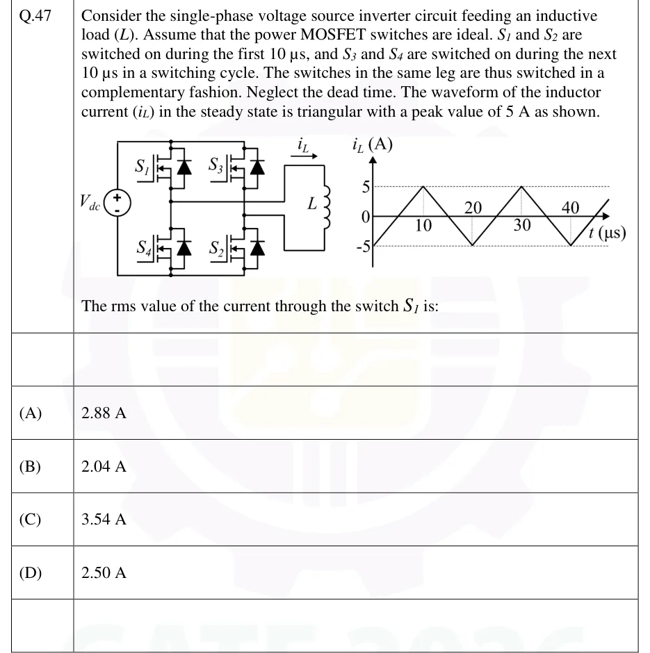
GATE 2026 EE question 47: Left: single-phase full bridge fed by a DC source V_dc (+ at top).Tap to open full size
Figure from the GATE 2026 EE paper. It is part of the question.
Figure description

Left: single-phase full bridge fed by a DC source V_dc (+ at top). Left leg has S1 (top) and S4 (bottom); right leg has S3 (top) and S2 (bottom). Each switch is a power MOSFET with an anti-parallel body diode. The inductive load L is connected between the midpoints of the two legs, with i_L marked as flowing from the left leg midpoint towards L. Right: plot of i_L (A) versus t (µs): a symmetric triangular wave starting at 0 at t = 0, peaks of +5 A, troughs of -5 A, dotted levels at +5 and -5, time marks at 10, 20, 30, 40 µs, so the period is 20 µs.

  1. (A)

    2.88 A

  2. (B)

    2.04 A

  3. (C)

    3.54 A

  4. (D)

    2.50 A

Answer and solution

ANSWER

The rms current through S1 is about 2.04 A, option (B).

Official answer: BSource: Official answer key, GATE 2026 EE (IIT Guwahati)

  1. The period is . S1 and S2 conduct for , so the duty ratio is . There is no phase control, so the firing angle is . The load voltage is in this interval and in the next 10 µs.

  2. From the plot, is a symmetric triangle between and . It rises linearly from to while , that is during . It falls linearly back to during the next 10 µs.

  3. While S1 and S2 are on, the left-leg midpoint is tied to the positive rail through S1, so the whole load current passes through S1. For it flows in the MOSFET channel. For it flows in the reverse direction through the channel or the body diode. In both cases for . For , S1 is off and its leg current flows through S4 or its diode, so .

  4. On the conducting interval, is linear from to with . Write with . Then

  5. The rms value over the full period is

  6. Substituting and gives This is option (B).

KEY IDEA

A switch carries the load current only while it is on. Compute the mean square of the load current over that interval and multiply by the duty ratio. A linear ramp from to has mean square . This holds whether the current flows in the MOSFET channel or its body diode.

WATCH OUT FOR

Counting only the positive half of the ramp, or dividing by the 10 µs conduction time instead of the full 20 µs period. Using (the sine-wave rule) for a triangle gives 2.50 A or 3.54 A, which are wrong. Dividing the ramp's rms by is correct. Forgetting the duty ratio gives 2.88 A.

From the GATE 2026 EE paper. Every question of this paper · Download the full paper · All 6 Inverters & PWM questions, with notes

More Inverters & PWM questions