
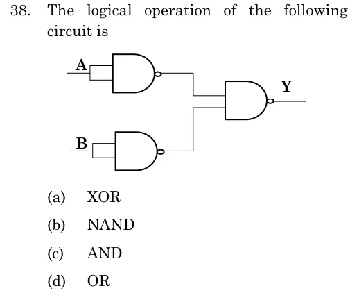
The logical operation of the following circuit is
 Tap to open full size
Figure description
Three NAND gates (AND shape with a bubble at the output). Input A is wired to both input pins of the first NAND gate (top left). Input B is wired to both input pins of the second NAND gate (bottom left). The output of the first NAND goes to the upper input of a third NAND gate and the output of the second NAND goes to its lower input. The third NAND gate's output is labelled Y.
- (A)
XOR
- (B)
NAND
- (C)
AND
- (D)
OR