
IAE Academy

GATE 2020 EC Q.32: solution and answer

GATE 2020 · ECQ.32 · 2 marks · MCQ

The band diagram of a p-type semiconductor with a band-gap of 1 eV is shown. Using this semiconductor, a MOS capacitor having of , of and a metal work function of is fabricated. There is no charge within the oxide. If the voltage across the capacitor is , the magnitude of depletion charge per unit area (in ) is
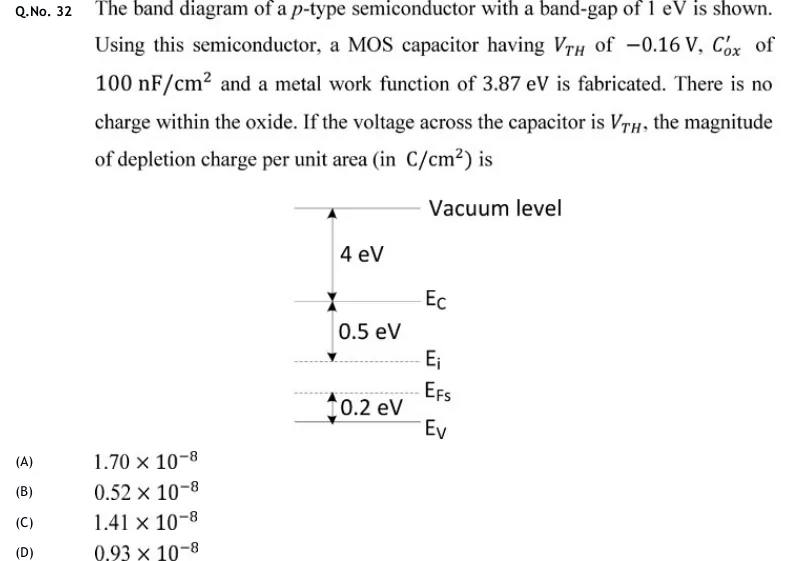
GATE 2020 EC question 32: Energy band diagram of a p-type semiconductor, vertical energy axis.Tap to open full size
Figure from the GATE 2020 EC paper. It is part of the question.
Figure description

Energy band diagram of a p-type semiconductor, vertical energy axis. Top to bottom: Vacuum level at top; a downward arrow of 4 eV from vacuum level to conduction band edge E_C (the electron affinity); below E_C a downward arrow of 0.5 eV to the intrinsic level E_i (dashed); below E_i the semiconductor Fermi level E_Fs (dashed), with an upward arrow of 0.2 eV from valence band edge E_V up to E_Fs; at the bottom, valence band edge E_V. Since band-gap is 1 eV and E_C - E_i = 0.5 eV, E_i - E_V is also 0.5 eV, so E_i - E_Fs = 0.5 - 0.2 = 0.3 eV.

  1. (A)

    1.70 x 10^-8

  2. (B)

    0.52 x 10^-8

  3. (C)

    1.41 x 10^-8

  4. (D)

    0.93 x 10^-8

Answer and solution

ANSWER

The magnitude of depletion charge per unit area is (Option A).

Official answer: ASource: Official answer key, GATE 2020 EC (IIT Delhi)

  1. From the band diagram, the electron affinity is (vacuum level to ).

  2. Using , , and band-gap : , so .

  3. Semiconductor work function: .

  4. Flat-band voltage: .

  5. Bulk potential magnitude: , so .

  6. Threshold-voltage relation for a p-substrate MOS capacitor with no oxide charge:

  7. Substituting: .

  8. , matching option A.

KEY IDEA

MOS threshold voltage relation for a p-type substrate: , where is obtained directly from the semiconductor band diagram (electron affinity plus the gap from down to ).

WATCH OUT FOR

Misreading the band diagram — adding instead of subtracting the 0.2 eV arrow (which points from up to ), giving eV instead of eV, or forgetting that the semiconductor work function must include the full gap from to (not just to ) when computing .

From the GATE 2020 EC paper. Every question of this paper · Download the full paper · All 7 MOS devices questions, with notes

More MOS devices questions