
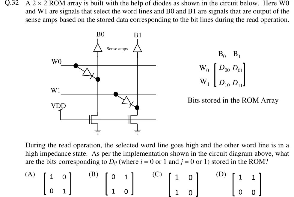
A ROM array is built with the help of diodes as shown in the circuit below. Here W0 and W1 are signals that select the word lines and B0 and B1 are signals that are output of the sense amps based on the stored data corresponding to the bit lines during the read operation.
[Figure: diode ROM array; beside it the matrix of bits stored in the ROM array, rows , columns : ]
During the read operation, the selected word line goes high and the other word line is in a high impedance state. As per the implementation shown in the circuit diagram above, what are the bits corresponding to (where or and or ) stored in the ROM?
 Tap to open full size
Figure description
Two horizontal word lines, W0 (top) and W1 (below it), cross two vertical bit lines, B0 (left) and B1 (right). At the top of each bit line is an upward-pointing buffer triangle (labelled 'Sense amps') whose output is labelled B0 and B1. Diode 1: its anode connects to W0 at a dot to the left of B0, and its cathode connects to the B0 bit line at a dot just below W0. The diode symbol points from W0 toward B0. Diode 2: its anode connects to W1 at a dot between B0 and B1, and its cathode connects to the B1 bit line just below W1. There is no diode between W0 and B1, and none between W1 and B0. At the bottom of each bit line is an n-channel MOSFET. Its drain is on the bit line and its source goes to ground. A horizontal line labelled VDD drives the gates of both MOSFETs, so both are always on and act as pull-down loads on the bit lines. To the right is the matrix 'Bits stored in the ROM Array': row W0 = [D00 D01], row W1 = [D10 D11], columns B0 and B1.
- (A)
- (B)
- (C)
- (D)