
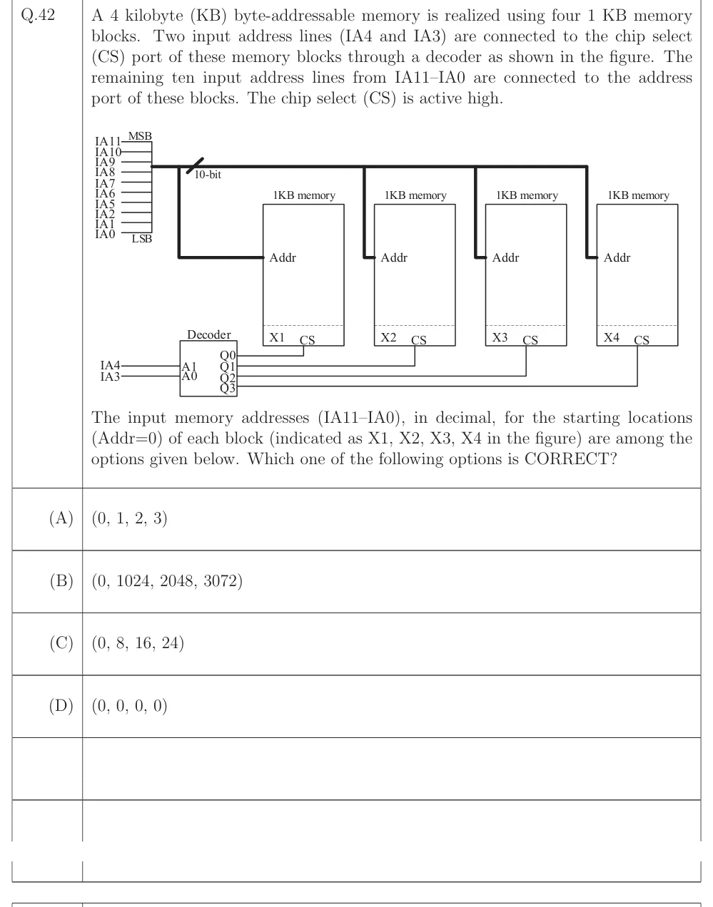
A 4 kilobyte (KB) byte-addressable memory is realized using four 1 KB memory blocks. Two input address lines (IA4 and IA3) are connected to the chip select (CS) port of these memory blocks through a decoder as shown in the figure. The remaining ten input address lines from IA11–IA0 are connected to the address port of these blocks. The chip select (CS) is active high.
The input memory addresses (IA11–IA0), in decimal, for the starting locations (Addr=0) of each block (indicated as X1, X2, X3, X4 in the figure) are among the options given below. Which one of the following options is CORRECT?
 Tap to open full size
Figure description
12 address lines IA11 (MSB) down to IA0 (LSB) enter from the left. The upper 10 lines actually used for addressing (all lines except IA4 and IA3) are bundled as a 10-bit bus labelled '10-bit' and fed to the 'Addr' input port of each of four 1KB memory blocks, labelled (left to right) with data-output/name X1, X2, X3, X4, each also having a CS (chip select) pin. IA4 and IA3 are instead routed down into a 2-to-4 decoder block: inputs A1 = IA4, A0 = IA3; outputs Q0, Q1, Q2, Q3 (top to bottom). Q0 connects to the CS of the first (X1) memory block, Q1 to the CS of the second (X2) block, Q2 to the CS of the third (X3) block, and Q3 to the CS of the fourth (X4) block, each via a horizontal wire running across to that block's CS pin. CS is active-high.
- (A)
(0, 1, 2, 3)
- (B)
(0, 1024, 2048, 3072)
- (C)
(0, 8, 16, 24)
- (D)
(0, 0, 0, 0)